
Tt nano HAT b2

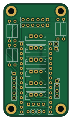
About the Tt nano HAT b2
Tt nano HAT b2 is an open source AVR/Arduino PCB design by vektorious, published on GitHub under the CC-BY-SA-4.0 license. It is a 2-layer board measuring 34 × 59 mm, with 21 components from 9 distinct parts.
Its main chip is the Arduino_Nano_v3.x, from the AVR/Arduino family. By type, the board carries 12 connectors, 8 resistors and 1 module.
It belongs with the dev boards & breakouts designs in this gallery.
From the project
Everything you need to build a test tube or flow-through photometer
For full project details see the main README.
First version of a Arduino Nano HAT to connect multiple photometer cells. It works BUT.
Problems: - jst connectors too close together
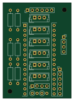
Second version of the Arduino Nano HAT. It looks better and works BUT.
Problems: - connections/annotation screwed up.
PCB that fits the opt101 and a potentiometer to set the sensitivity of the sensor. Works great and fits perfectly into the housing of the measurement cells.

Main components on the Tt nano HAT b2
Tt nano HAT b2 bill of materials (BOM)
21 components, 9 distinct parts — part numbers from the project's BOM.
| Qty | Part | Footprint | Refs |
|---|---|---|---|
| 1 | Arduino_Nano_v3.x | Arduino_Nano2 | A1 |
| 1 | 22-03-2041 Conn_01x04_Male Molex | PinHeader_1x04_P2.54mm_Vertical | J1 |
| 2 | 22-03-2061 Conn_01x06_Male Molex | PinHeader_1x06_P2.54mm_Vertical | J2, J10 |
| 1 | M20-7820446 Conn_01x04_Female Harwin | PinSocket_1x04_P2.54mm_Vertical | J3 |
| 6 | 455-1612 Conn_01x03_Male JST | JST_EH_B03B-EH-A_1x03_P2.50mm_Vertical | J4, J5, J6, J7, J8, J9 |
| 1 | Conn_01x02_Male | PinHeader_1x02_P2.54mm_Vertical | J11 |
| 1 | Conn_01x06_Male | PinHeader_1x06_P2.54mm_Vertical | J12 |
| 2 | ROX3SJ10K R TE Connectivity | R_Axial_DIN0207_L6.3mm_D2.5mm_P2.54mm_Vertical | R1, R8 |
| 6 | C14220RJL R TE Connectivity | R_Axial_DIN0207_L6.3mm_D2.5mm_P10.16mm_Horizontal | R2, R3, R4, R5, R6, R7 |
Tt nano HAT b2 design files
The KiCad project lives in the vektorious/test_tube_photometer repository on GitHub; these links point at the commit this page was built from.
Tt nano HAT b2: common questions
What microcontroller does the Tt nano HAT b2 use?
The Tt nano HAT b2 is built around the Arduino_Nano_v3.x, from the AVR/Arduino family.
How big is the Tt nano HAT b2?
The Tt nano HAT b2 measures 34 × 59 mm, has 2 copper layers and is 1.6 mm thick.
How many components are on the Tt nano HAT b2?
21 components, from 9 distinct parts, with part numbers taken from the project's own BOM. The full bill of materials is listed on this page.
Where can I download the Tt nano HAT b2 design files?
From the vektorious/test_tube_photometer repository on GitHub, which has the KiCad layout and the BOM; the links under Design files point to each one.
Can I use the Tt nano HAT b2 design in my own project?
Yes, under the terms of its CC-BY-SA-4.0 license, which vektorious chose for the repository.
Can I test firmware for the Tt nano HAT b2 without the hardware?
Yes. HardLabs builds a simulation of the board from its netlist and BOM, so you can run and debug AVR/Arduino firmware against it before you order a PCB.
More boards in test_tube_photometer

Similar boards
 AVR/Arduino
Magspoof
samyk
35 × 29 mm11 parts2LNo license4.2k AVR/Arduino
Redox keyboard
mattdibi
162.2 × 126.5 mm77 parts2LMIT2.0k AVR/Arduino
Labrador
espotek-org
36.8 × 34.7 mm75 parts2LNo license1.2k AVR/Arduino
V4
stuartpittaway
30 × 50 mm38 parts2LCC-BY-NC-4.01.1k AVR/Arduino
ModuleV450
30 × 61.4 mm39 parts2LCC-BY-NC-4.01.1k AVR/Arduino
Discipline
coseyfannitutti
304.9 × 122.8 mm170 parts2LCC-BY-NC-4.01.0k