
Kinesis

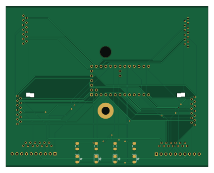
About the Kinesis PCB
Kinesis is an open source RP2040/RP2350 PCB design by yakloinsteak, published on GitHub under the CC-BY-SA-4.0 license. It is a 2-layer board measuring 108 × 86 mm, with 17 components from 11 distinct parts.
Its main chip is the PROMICRO_RP2040, from the RP2040/RP2350 family. By type, the board carries 8 connectors, 4 LEDs, 4 resistors and 1 IC.
It belongs with the keyboards designs in this gallery.
From the project
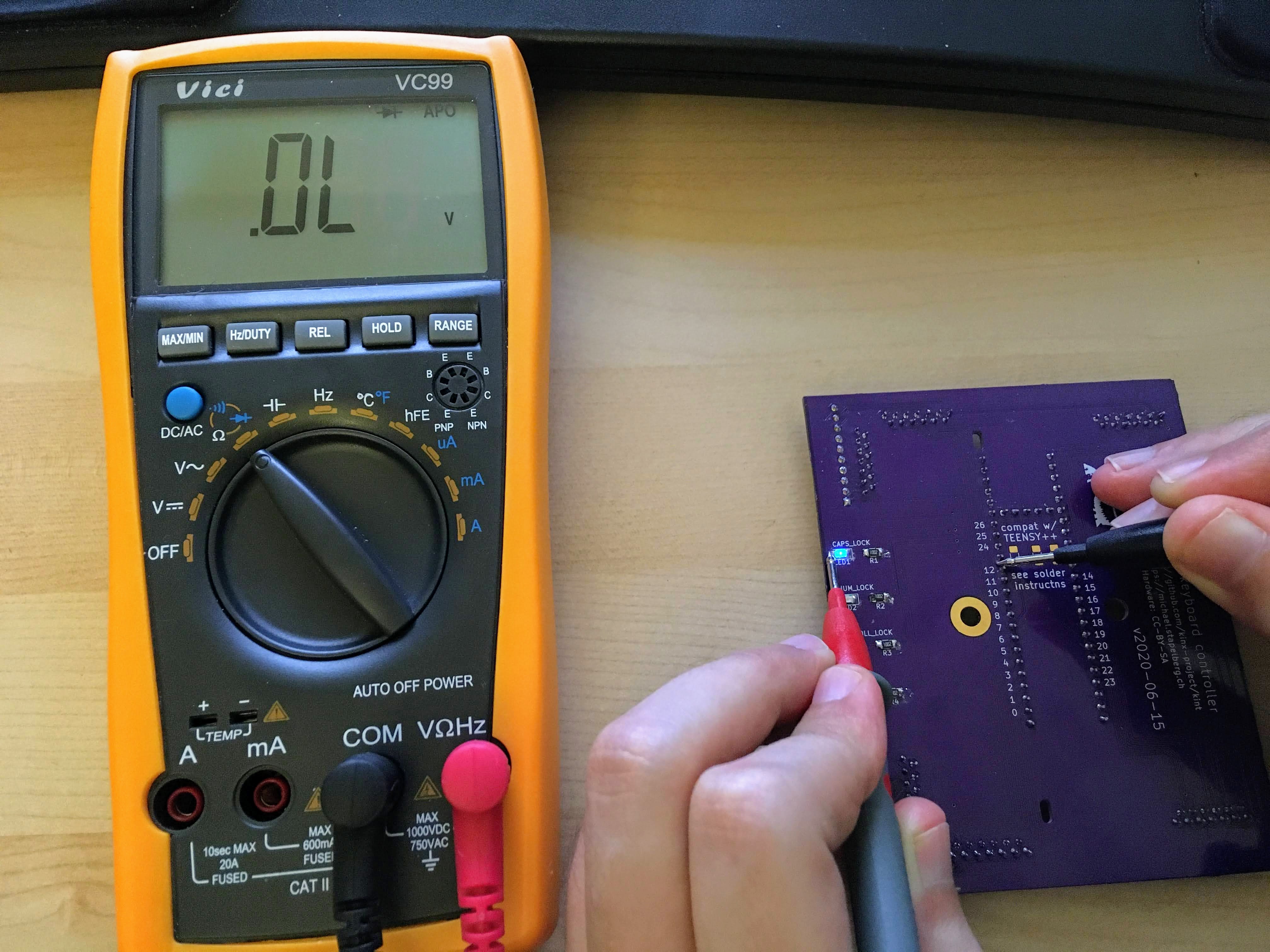
rp2040 port of kint for the teensie
(Photo shows the previous Teensy-based revision.)
The kinRP2040 keyboard controller is a replacement for your Kinesis Advantage or Advantage 2 ergonomic keyboards. It is a derivative of Michael Stapelberg's kinT that replaces the Teensy microcontroller with a generic, off-the-shelf ProMicro RP2040 module, sidestepping Teensy availability and discontinuation concerns.
Main components on the Kinesis
Kinesis bill of materials (BOM)
17 components, 11 distinct parts.
| Qty | Part | Footprint | Refs |
|---|---|---|---|
| 1 | PROMICRO_RP2040 | PROMICRO_RP2040 | U1 |
| 1 | 39-53-2135 THUMB_RIGHT_SPC_KB600 | 39-53-2135 | J1 |
| 1 | 39-53-2135 LEFT_13_LT | 39-53-2135 | J2 |
| 1 | 39-53-2135 TOP_LEFT | 39-53-2135 | J3 |
| 1 | 39-53-2135 TOP_RIGHT | 39-53-2135 | J4 |
| 1 | 39-53-2135 THUMB_LEFT_BAK | PinHeader_1x10_P2.54mm_Vertical | J5 |
| 1 | 39-53-2135 THUMB_RIGHT_SPC | PinHeader_1x10_P2.54mm_Vertical | J6 |
| 1 | 39-53-2135 RIGHT_13_DOWN | 39-53-2135 | J7 |
| 1 | 39-53-2135 THUMB_LEFT_BAK_KB600 | 39-53-2135 | J8 |
| 4 | APT3216QBC/D LEDSML1206 | LED_1206_3216Metric_Pad1.42x1.75mm_HandSolder | LED1, LED2, LED3, LED4 |
| 4 | CRCW120610K0FKEAC 10K | R_1206_3216Metric_Pad1.42x1.75mm_HandSolder | R1, R2, R3, R4 |
Kinesis design files
The KiCad project lives in the yakloinsteak/kinesis repository on GitHub; these links point at the commit this page was built from.
- Layoutkicad/kint.kicad_pcb
- Schematickicad/kint.kicad_sch
Kinesis: common questions
What microcontroller does the Kinesis use?
The Kinesis is built around the PROMICRO_RP2040, from the RP2040/RP2350 family.
How big is the Kinesis PCB?
The Kinesis measures 108 × 86 mm, has 2 copper layers and is 1.6 mm thick.
How many components are on the Kinesis?
17 components, from 11 distinct parts. The full bill of materials is listed on this page.
Where can I download the Kinesis design files?
From the yakloinsteak/kinesis repository on GitHub, which has the KiCad layout and the schematic; the links under Design files point to each one.
Can I use the Kinesis design in my own project?
Yes, under the terms of its CC-BY-SA-4.0 license, which yakloinsteak chose for the repository.
Can I test firmware for the Kinesis without the hardware?
Yes. HardLabs builds a simulation of the board from its netlist and BOM, so you can run and debug RP2040/RP2350 firmware against it before you order a PCB.
Similar boards
 RP2040/RP2350
OSO-BOOK-C1
joeycastillo
85 × 115 mm29 parts2LCC-BY-SA-4.08.1k RP2040/RP2350
Corne chocolate
foostan
277.2 × 107.5 mm164 parts2LCC-BY-4.07.7k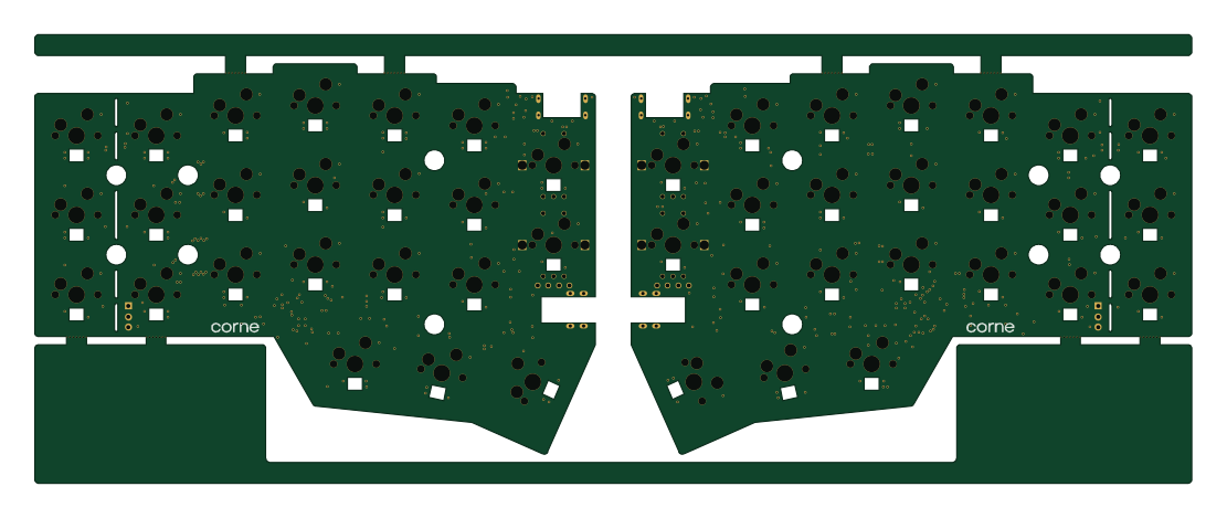 RP2040/RP2350
Corne cherry
277.2 × 107.5 mm164 parts2LCC-BY-4.07.7k RP2040/RP2350
Jitx design
gusmanb
55.5 × 65 mm26 parts4LGPL-3.05.0k RP2040/RP2350
LogicAnalyzer
57 × 55.2 mm6 parts2LGPL-3.05.0k RP2040/RP2350
Main
google
98 × 71 mm102 parts2LApache-2.02.9k