
Moved grid attempt

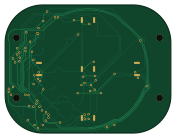
About the Moved grid attempt PCB
Moved grid attempt is an open source ESP32 PCB design by 0x616c6f6e, published on GitHub. It is a 2-layer board measuring 44 × 34 mm, with 23 components from 14 distinct parts.
Its main chip is the ESP32-S31NRV16, from the ESP32 family. By type, the board carries 13 resistors, 5 switches, 3 capacitors, 1 IC and 1 connector.
From the project
源电路为 AT42QT2120 + TCA6408A;目标为单颗 CH32V006F8U6。before/ 是本次操作前的原文件备份;candidate/ 是工作候选文件。以 hardware-controls 根目录中的最终工程为准,不要从这里的中间 PCB 导出生产文件。
源电路为 AT42QT2120 + TCA6408A;目标为单颗 CH32V006F8U6。before/ 是本次操作前的原文件备份;candidate/ 是工作候选文件。以 hardware-controls 根目录中的最终工程为准,不要从这里的中间 PCB 导出生产文件。
design.json 记录本版原理图 UUID、元件、实际 KiCad 顶视坐标、MCU 引脚与 FPC 接口。这里的坐标是实际 PCB 坐标,不能直接交给历史脚本中采用 44-x 镜像约定的机械生成器。
检查报告以 final-erc.json、final-drc.json、validation.json 为准;带 pre-route / routed / fanout / grid 字样的文件仅用于迁移过程诊断。模型预览用于检查元件体积与布局,不代替整机 FreeCAD 装配的干涉验证。
Main components on the Moved grid attempt
Moved grid attempt bill of materials (BOM)
23 components, 14 distinct parts — part numbers from the project's BOM.
| Qty | Part | Footprint | Refs |
|---|---|---|---|
| 1 | ESP32-S31NRV16 CH32V006F8U6 Espressif | CH32V006_QFN20 | U1 |
| 1 | HC-FPC-05-10-12RLTAG | HCTL_FPC12 | J1 |
| 5 | SKSWCEE010 | SKSW_3x2 | SW1, SW2, SW3, SW4, SW5 |
| 1 | GRM0335C1H240JA01D 100nF Murata | C0402 | C1 |
| 1 | GRM0335C1H270JA01D 1uF Murata | C0402 | C2 |
| 1 | 100nF Murata | C0402 | C3 |
| 3 | 0201WMF0000TCE 1k UniOhm | R0402 | R1, R2, R3 |
| 2 | 0201WMF0000TCE 4.7k UniOhm | R0402 | R4, R5 |
| 1 | 0201WMF4990TCE 10k UniOhm | R0402 | R6 |
| 2 | 10k | R0402 | R7, R14 |
| 1 | 0201WMF0000TCE 0R UniOhm | R0402 | R8 |
| 1 | 0201WMF0000TCE 47k UniOhm | R0402 | R9 |
| 1 | 0201WMF1002TCE 47k UniOhm | R0402 | R10 |
| 2 | 47k | R0402 | R11, R12 |
Moved grid attempt design files
The KiCad project lives in the 0x616c6f6e/esp32s31-mp3 repository on GitHub; these links point at the commit this page was built from.
Moved grid attempt: common questions
What microcontroller does the Moved grid attempt use?
The Moved grid attempt is built around the ESP32-S31NRV16, from the ESP32 family.
How big is the Moved grid attempt PCB?
The Moved grid attempt measures 44 × 34 mm, has 2 copper layers and is 0.8 mm thick.
How many components are on the Moved grid attempt?
23 components, from 14 distinct parts, with part numbers taken from the project's own BOM. The full bill of materials is listed on this page.
Where can I download the Moved grid attempt design files?
From the 0x616c6f6e/esp32s31-mp3 repository on GitHub, which has the KiCad layout and the BOM; the links under Design files point to each one.
Can I use the Moved grid attempt design in my own project?
The repository has no license, so all rights stay with 0x616c6f6e. Use it as a reference, and ask the author before reusing the design.
Can I test firmware for the Moved grid attempt without the hardware?
Yes. HardLabs builds a simulation of the board from its netlist and BOM, so you can run and debug ESP32 firmware against it before you order a PCB.
More boards in esp32s31-mp3
 ESP32
ESP32Q2-v2
46 × 76 mm192 parts6LNo license0 ESP32
ESP32ProPrj esp32s31-mp4 2026-09-22
46 × 76 mm135 parts6LNo license0 ESP32
ESP32Mainboard model reference
46 × 76 mm135 parts6LNo license0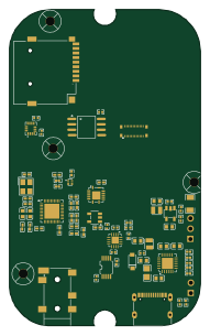 ESP32
ESP32Q2-v2-placement
46 × 76 mm126 parts6LNo license0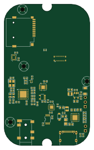 ESP32
ESP32Base
46 × 76 mm119 parts6LNo license0 ESP32
ESP32Core reference
22 × 30 mm47 parts4LNo license0 ESP32
ESP32Controls power pullup base
44 × 34 mm26 parts2LNo license0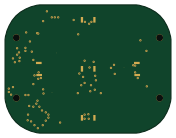 ESP32
ESP32Grid trunks attempt
44 × 34 mm23 parts2LNo license0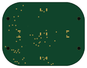 RISC-V
Controls
44 × 34 mm23 parts2LNo license0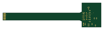
Am213-fpc adapter
87 × 22 mm16 parts2LNo license0
Similar boards
 ESP32
ESP32Open Book Abridged Edition
joeycastillo
85 × 115 mm65 parts2LCC-BY-SA-4.08.1k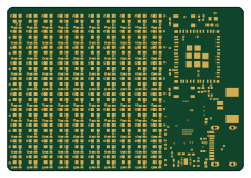 ESP32
ESP32Badge
atopile
56.3 × 39 mm239 parts4LMIT4.0k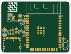 ESP32
ESP32Esp32 minimal
36.2 × 26.8 mm20 parts2LMIT4.0k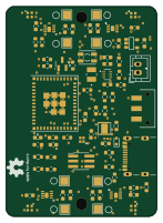 ESP32
ESP32Racer
StuckAtPrototype
36 × 50.2 mm70 parts4LApache-2.03.8k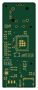 ESP32
ESP32Controller
29 × 74 mm58 parts4LApache-2.03.8k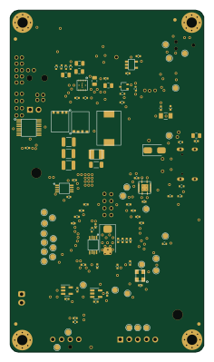 ESP32
ESP32Bitaxe
skot
56.5 × 99.8 mm86 parts4LCERN-OHL-S-2.01.4k