
PacSat JTAG Interface

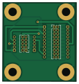
About the PacSat JTAG Interface PCB
PacSat JTAG Interface is an open source PCB design by AMSAT-NA, published on GitHub. It is a 2-layer board measuring 28.1 × 29.9 mm, with 6 components from 4 distinct parts.
It belongs with the usb & debug tools designs in this gallery.
PacSat JTAG Interface bill of materials (BOM)
6 components, 4 distinct parts — part numbers from the project's BOM.
| Qty | Part | Footprint | Refs |
|---|---|---|---|
| 1 | CONN_02X05 | PinHeader_2x05_P1.27mm_Vertical | J1 |
| 1 | CONN_02X05 | PinHeader_2x10_P1.27mm_Vertical | J2 |
| 2 | Conn_01x05_Pin | PinHeader_1x05_P1.27mm_Vertical | J3, J4 |
| 2 | Conn_01x10_Pin | PinHeader_1x10_P1.27mm_Vertical | J5, J6 |
PacSat JTAG Interface design files
The KiCad project lives in the AMSAT-NA/PacSatDocs repository on GitHub; these links point at the commit this page was built from.
PacSat JTAG Interface: common questions
How big is the PacSat JTAG Interface PCB?
The PacSat JTAG Interface measures 28.1 × 29.9 mm, has 2 copper layers and is 1.6 mm thick.
How many components are on the PacSat JTAG Interface?
6 components, from 4 distinct parts, with part numbers taken from the project's own BOM. The full bill of materials is listed on this page.
Where can I download the PacSat JTAG Interface design files?
From the AMSAT-NA/PacSatDocs repository on GitHub, which has the KiCad layout, the schematic and the BOM; the links under Design files point to each one.
Can I use the PacSat JTAG Interface design in my own project?
The repository has no license, so all rights stay with AMSAT-NA. Use it as a reference, and ask the author before reusing the design.
More boards in PacSatDocs
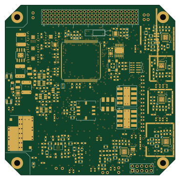
PacSat Alpha Board
92 × 92 mm341 parts6LNo license4
PacSat Alpha Board
92 × 92 mm341 parts6LNo license4
PacSat Alpha Board
92 × 92 mm341 parts6LNo license4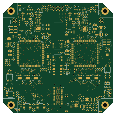
Rtihu
92 × 92 mm295 parts4LNo license4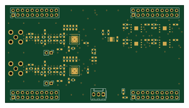
AX5043 Booster for Hercules Launchpad
94 × 51 mm88 parts2LNo license4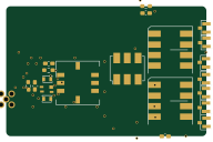
Power Devider
47.8 × 31 mm38 parts2LNo license4
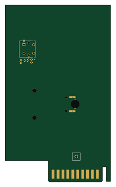
AX5043 RX
24.6 × 22.4 mm34 parts4LNo license4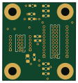
PacSat JTAG RevA
28.1 × 29.8 mm19 parts2LNo license4
Similar boards
XG Station Power
osy
54.3 × 91 mm9 parts2LCC-BY-4.0703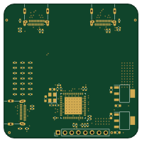
USB Hub Test
50 × 50 mm85 parts4LCC-BY-4.0703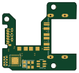
FW-EC-DongleHiderPlus
LeoDJ
28.2 × 26.1 mm14 parts4LCERN-OHL-W-2.0490
Adapter tsop48
bbogush
48 × 33 mm3 parts2LGPL-3.0389
Adapter tsop48 solder
48 × 33 mm3 parts2LGPL-3.0389
Adapter soic8 solder
48 × 20 mm3 parts2LGPL-3.0389