
HACKPAD

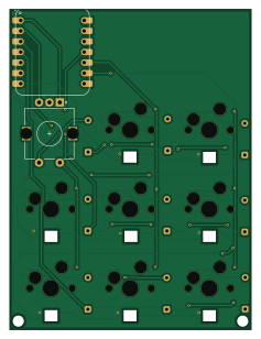
About the HACKPAD PCB
HACKPAD is an open source RP2040/RP2350 PCB design by ankitanandchoudhary2006-eng, published on GitHub. It is a 2-layer board measuring 58 × 77 mm, with 27 components from 5 distinct parts.
Its main chip is the XIAO-RP2040-DIP, from the RP2040/RP2350 family. By type, the board carries 17 diodes, 9 switches and 1 IC.
It belongs with the keyboards designs in this gallery.
From the project
SO I make a 3x3 HACKPAD for myself . It is based on RP2040 and I tried it to make it compact as possible. It has a rotor Encoder as well . The PCB was designed on kicad and the CAD was designed on Fusion. It has diodes to prevent ghosting and LEDs as well.
SO I make a 3x3 HACKPAD for myself . It is based on RP2040 and I tried it to make it compact as possible. It has a rotor Encoder as well . The PCB was designed on kicad and the CAD was designed on Fusion. It has diodes to prevent ghosting and LEDs as well.
First Solder the Diodes and the HotSwap then Solder the LEDS after that Solder the Xiao RP2040 Board and at the END solder the Rotor Encoder also before plugging it . Check if there is any mis-connection , shot or disconnection.
Main components on the HACKPAD
HACKPAD bill of materials (BOM)
27 components, 5 distinct parts.
| Qty | Part | Footprint | Refs |
|---|---|---|---|
| 1 | XIAO-RP2040-DIP | XIAO-RP2040-DIP | U1 |
| 1 | RotaryEncoder_Switch_MP | RotaryEncoder_Alps_EC11E-Switch_Vertical_H20mm | SW0 |
| 8 | SW_Push | MX100H | SW1, SW2, SW3, SW4, SW5, SW6, SW7, SW8 |
| 9 | 1N4148 | D_DO-35_SOD27_P7.62mm_Horizontal | D1, D2, D3, D4, D5, D6, D7, D8 +1 |
| 8 | SK6812-E | LED_SK6812-E | D10, D11, D12, D13, D14, D15, D16, D18 |
HACKPAD design files
The KiCad project lives in the ankitanandchoudhary2006-eng/HACKPAD repository on GitHub; these links point at the commit this page was built from.
- LayoutPCB/HACKPAD.kicad_pcb
- SchematicPCB/HACKPAD.kicad_sch
HACKPAD: common questions
What microcontroller does the HACKPAD use?
The HACKPAD is built around the XIAO-RP2040-DIP, from the RP2040/RP2350 family.
How big is the HACKPAD PCB?
The HACKPAD measures 58 × 77 mm, has 2 copper layers and is 1.6 mm thick.
How many components are on the HACKPAD?
27 components, from 5 distinct parts. The full bill of materials is listed on this page.
Where can I download the HACKPAD design files?
From the ankitanandchoudhary2006-eng/HACKPAD repository on GitHub, which has the KiCad layout and the schematic; the links under Design files point to each one.
Can I use the HACKPAD design in my own project?
The repository has no license, so all rights stay with ankitanandchoudhary2006-eng. Use it as a reference, and ask the author before reusing the design.
Can I test firmware for the HACKPAD without the hardware?
Yes. HardLabs builds a simulation of the board from its netlist and BOM, so you can run and debug RP2040/RP2350 firmware against it before you order a PCB.
Similar boards
 RP2040/RP2350
OSO-BOOK-C1
joeycastillo
85 × 115 mm29 parts2LCC-BY-SA-4.08.1k RP2040/RP2350
Corne chocolate
foostan
277.2 × 107.5 mm164 parts2LCC-BY-4.07.7k RP2040/RP2350
Corne cherry
277.2 × 107.5 mm164 parts2LCC-BY-4.07.7k RP2040/RP2350
Jitx design
gusmanb
55.5 × 65 mm26 parts4LGPL-3.05.0k RP2040/RP2350
LogicAnalyzer
57 × 55.2 mm6 parts2LGPL-3.05.0k RP2040/RP2350
Main
google
98 × 71 mm102 parts2LApache-2.02.9k