
Testgen

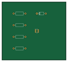
About the Testgen PCB
Testgen is an open source PCB design by AquaBeacon, published on GitHub under the Apache-2.0 license. It is a 2-layer board measuring 55 × 50 mm, with 6 components from 3 distinct parts.
Other key parts include the SOT-23-6. By type, the board carries 4 resistors, 1 IC and 1 diode.
From the project
回路図・PCB・製造ツール
LTspiceで検証済みの4回路(LTspice/ sim/notes.md 参照)をKiCadの回路図+PCBに実装したもの。 すべて ERC合格・意図ネットリスト照合合格・DRC 0違反/未配線0。
各フォルダの内容: .kicadsch / .kicadpcb / .kicadpro、schematic.pdf、 render.png(3Dレンダ)、gerbers/(ガーバー+ドリル)、erc.rpt / drc.rpt、.net、 bom.csv(部品表: Value/Footprintでグループ化)。 datasheets/` に発注前確認で参照した一次資料(2SK4017東芝純正データシート)を同梱。
発注・組立時は ORDERING.md(4基板統合発注リスト+代替品情報)と BRINGUP.md(組立順序・通電手順・シミュ由来の期待測定値)を参照。 全体システム(Pico/SPRESENSE/テザー)への組み込みは SYSTEMINTEGRATION.md** (設計書とのギャップ分析・J2↔GPIO対応表)を参照。
Main components on the Testgen
Testgen bill of materials (BOM)
6 components, 3 distinct parts — part numbers from the project's BOM.
| Qty | Part | Footprint | Refs |
|---|---|---|---|
| 1 | SOT-23-6 | SOT-23-6 | U1 |
| 1 | D_DO-35_SOD27_P7.62mm_Horizontal | D_DO-35_SOD27_P7.62mm_Horizontal | D1 |
| 4 | R_Axial_DIN0207_L6.3mm_D2.5mm_P10.16mm_Horizontal | R_Axial_DIN0207_L6.3mm_D2.5mm_P10.16mm_Horizontal | R1, R2, R3, R4 |
Testgen design files
The KiCad project lives in the AquaBeacon/hardware repository on GitHub; these links point at the commit this page was built from.
Testgen: common questions
How big is the Testgen PCB?
The Testgen measures 55 × 50 mm, has 2 copper layers and is 1.6 mm thick.
How many components are on the Testgen?
6 components, from 3 distinct parts, with part numbers taken from the project's own BOM. The full bill of materials is listed on this page.
Where can I download the Testgen design files?
From the AquaBeacon/hardware repository on GitHub, which has the KiCad layout, the schematic and the BOM; the links under Design files point to each one.
Can I use the Testgen design in my own project?
Yes, under the terms of its Apache-2.0 license, which AquaBeacon chose for the repository.
More boards in hardware
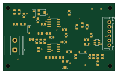
RX advanced mini
60 × 36 mm45 parts2LApache-2.00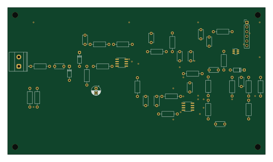
RX advanced
140 × 80 mm43 parts2LApache-2.00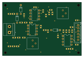
RX improved mini
68 × 46 mm41 parts2LApache-2.00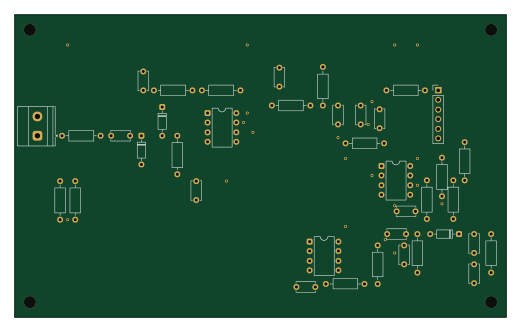
RX improved
130 × 80 mm39 parts2LApache-2.00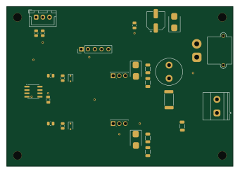
TX advanced
85 × 60 mm28 parts2LApache-2.00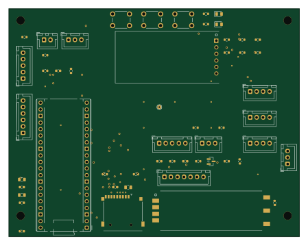 RP2040/RP2350
PARENT MAIN
112 × 88 mm24 parts2LApache-2.00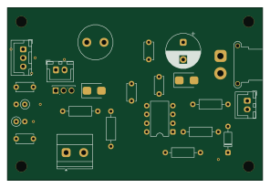
TX improved
74 × 50 mm24 parts2LApache-2.00 RP2040/RP2350
CHILD MAIN
104 × 88 mm22 parts2LApache-2.00
CHILD PWR
62 × 70 mm15 parts2LApache-2.00
PARENT PWR
100 × 84 mm13 parts2LApache-2.00