
PARENT MAIN

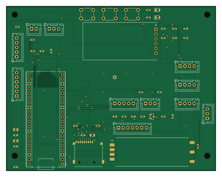
About the PARENT MAIN PCB
PARENT MAIN is an open source RP2040/RP2350 PCB design by AquaBeacon, published on GitHub under the Apache-2.0 license. It is a 2-layer board measuring 112 × 88 mm, with 24 components from 18 distinct parts.
Its main chip is the Pico 2 W, from the RP2040/RP2350 family.
From the project
回路図・PCB・製造ツール
LTspiceで検証済みの4回路(LTspice/ sim/notes.md 参照)をKiCadの回路図+PCBに実装したもの。 すべて ERC合格・意図ネットリスト照合合格・DRC 0違反/未配線0。
各フォルダの内容: .kicadsch / .kicadpcb / .kicadpro、schematic.pdf、 render.png(3Dレンダ)、gerbers/(ガーバー+ドリル)、erc.rpt / drc.rpt、.net、 bom.csv(部品表: Value/Footprintでグループ化)。 datasheets/` に発注前確認で参照した一次資料(2SK4017東芝純正データシート)を同梱。
発注・組立時は ORDERING.md(4基板統合発注リスト+代替品情報)と BRINGUP.md(組立順序・通電手順・シミュ由来の期待測定値)を参照。 全体システム(Pico/SPRESENSE/テザー)への組み込みは SYSTEMINTEGRATION.md** (設計書とのギャップ分析・J2↔GPIO対応表)を参照。
PARENT MAIN bill of materials (BOM)
24 components, 18 distinct parts — part numbers from the project's BOM.
| Qty | Part | Footprint | Refs |
|---|---|---|---|
| 5 | 100n | C_0603_1608Metric | C_D1, C_D2, C_SD1, C_V3b, C_V5b |
| 3 | 10u | C_0805_2012Metric | C_SD2, C_V3, C_V5 |
| 1 | NEO_M9N | JST_XH_B5B-XH-A_1x05_P2.50mm_Vertical | J_GNSS1 |
| 1 | I2C_FROM_PPWR | JST_XH_B5B-XH-A_1x05_P2.50mm_Vertical | J_I2CP |
| 1 | NHD_C0216CiZ | JST_XH_B7B-XH-A_1x07_P2.50mm_Vertical | J_LCD1 |
| 1 | LIS3MDL | JST_XH_B4B-XH-A_1x04_P2.50mm_Vertical | J_MAG1 |
| 1 | MS5837 | JST_XH_B4B-XH-A_1x04_P2.50mm_Vertical | J_PRS1 |
| 1 | PWR_FROM_PPWR | JST_XH_B6B-XH-A_1x06_P2.50mm_Vertical | J_PWR1 |
| 1 | DS3231_ZS042 | DS3231_ZS042 | J_RTC1 |
| 1 | TO_SPRESENSE_EXT_3V3 | JST_XH_B3B-XH-A_1x03_P2.50mm_Vertical | J_SPR1 |
| 1 | CELSIUS_TEMP | JST_XH_B4B-XH-A_1x04_P2.50mm_Vertical | J_TEMP1 |
| 1 | TETHER | JST_XH_B3B-XH-A_1x03_P2.50mm_Vertical | J_TETH1 |
| 1 | TO_PTX_PWM | JST_XH_B2B-XH-A_1x02_P2.50mm_Vertical | J_TX1 |
| 1 | TO_PTX_TEMP | JST_XH_B3B-XH-A_1x03_P2.50mm_Vertical | J_TXT1 |
| 1 | Pico 2 W | RaspberryPi_Pico_Common_THT | PICO1 |
| 1 | 120_DNP | R_0603_1608Metric | R_TRMD1 |
| 1 | microSD | microSD_TF-01A | SD1 |
| 1 | W_RS485_DATA | Waveshare_TTL_RS485_C | U_485D1 |
PARENT MAIN design files
The KiCad project lives in the AquaBeacon/hardware repository on GitHub; these links point at the commit this page was built from.
PARENT MAIN: common questions
What microcontroller does the PARENT MAIN use?
The PARENT MAIN is built around the Pico 2 W, from the RP2040/RP2350 family.
How big is the PARENT MAIN PCB?
The PARENT MAIN measures 112 × 88 mm, has 2 copper layers and is 1.6 mm thick.
How many components are on the PARENT MAIN?
24 components, from 18 distinct parts, with part numbers taken from the project's own BOM. The full bill of materials is listed on this page.
Where can I download the PARENT MAIN design files?
From the AquaBeacon/hardware repository on GitHub, which has the KiCad layout, the schematic and the BOM; the links under Design files point to each one.
Can I use the PARENT MAIN design in my own project?
Yes, under the terms of its Apache-2.0 license, which AquaBeacon chose for the repository.
Can I test firmware for the PARENT MAIN without the hardware?
Yes. HardLabs builds a simulation of the board from its netlist and BOM, so you can run and debug RP2040/RP2350 firmware against it before you order a PCB.
More boards in hardware
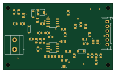
RX advanced mini
60 × 36 mm45 parts2LApache-2.00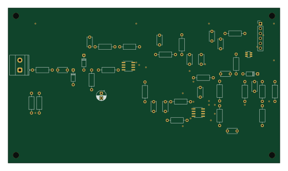
RX advanced
140 × 80 mm43 parts2LApache-2.00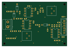
RX improved mini
68 × 46 mm41 parts2LApache-2.00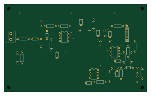
RX improved
130 × 80 mm39 parts2LApache-2.00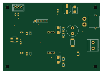
TX advanced
85 × 60 mm28 parts2LApache-2.00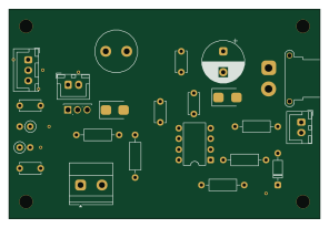
TX improved
74 × 50 mm24 parts2LApache-2.00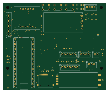 RP2040/RP2350
CHILD MAIN
104 × 88 mm22 parts2LApache-2.00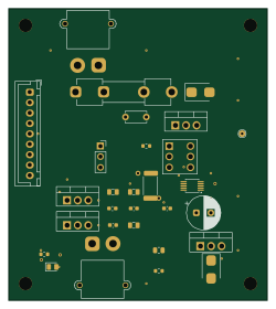
CHILD PWR
62 × 70 mm15 parts2LApache-2.00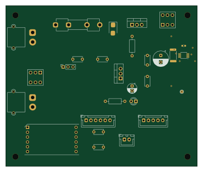
PARENT PWR
100 × 84 mm13 parts2LApache-2.00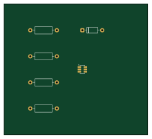
Testgen
55 × 50 mm6 parts2LApache-2.00
Similar boards
 RP2040/RP2350
Open Book Abridged Edition
joeycastillo
85 × 115 mm29 parts2LCC-BY-SA-4.08.1k RP2040/RP2350
Corne
foostan
277.2 × 107.5 mm164 parts2LCC-BY-4.07.7k RP2040/RP2350
Corne
277.2 × 107.5 mm164 parts2LCC-BY-4.07.7k RP2040/RP2350
LogicAnalyzer
gusmanb
57 × 55.2 mm6 parts2LGPL-3.05.0k RP2040/RP2350
Jitx design
55.5 × 65 mm26 parts4LGPL-3.05.0k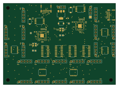 RP2040/RP2350
Main
google
98 × 71 mm102 parts2LApache-2.02.9k