
Panel

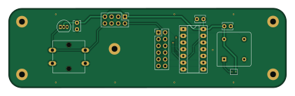
About the Panel PCB
Panel is an open source PCB design by atarola, published on GitHub. It is a 2-layer board measuring 105.4 × 30.1 mm, with 9 components from 7 distinct parts.
Other key parts include the DS1813-19 and SN74HC393N. By type, the board carries 3 capacitors, 2 ICs, 2 connectors, 1 crystal and 1 switch.
It belongs with the retro computing designs in this gallery.
From the project
Code for my 6502 build
compy6502 is an early-stage 6502 homebrew computer project. The long-term goal is to build enough hardware and firmware to run Tetris on the machine.
The design follows the spirit of Ben Eater-style breadboard/modular 6502 systems for simplicity and debuggability, but uses a different memory map based on the MMU/address-decoder architecture in docs/mmu.png.
The repo currently includes KiCad hardware designs, early ROM bring-up firmware, build/write scripts, emulator test scaffolding, and architecture reference images in docs/.
Main components on the Panel
Panel bill of materials (BOM)
9 components, 7 distinct parts.
| Qty | Part | Footprint | Refs |
|---|---|---|---|
| 1 | DS1813-19 | TO-92_Inline | U1 |
| 1 | SN74HC393N | DIP-14_W7.62mm_Socket_LongPads | U2 |
| 1 | 16 mhz | Oscillator_DIP-8 | Y1 |
| 1 | Speed Selector | PinHeader_2x06_P2.54mm_Vertical | J2 |
| 1 | Conn_02x04_Counter_Clockwise | PinHeader_2x04_P2.54mm_Vertical | J8 |
| 1 | Reset Button | SW_SPST_Omron_B3F-40xx | SW1 |
| 3 | 0.1u | C_Disc_D3.8mm_W2.6mm_P2.50mm | C6, C7, C8 |
Panel design files
The KiCad project lives in the atarola/compy6502 repository on GitHub; these links point at the commit this page was built from.
- Layoutkicad/panel/panel.kicad_pcb
- Schematickicad/panel/panel.kicad_sch
Panel: common questions
How big is the Panel PCB?
The Panel measures 105.4 × 30.1 mm, has 2 copper layers and is 1.6 mm thick.
How many components are on the Panel?
9 components, from 7 distinct parts. The full bill of materials is listed on this page.
Where can I download the Panel design files?
From the atarola/compy6502 repository on GitHub, which has the KiCad layout and the schematic; the links under Design files point to each one.
Can I use the Panel design in my own project?
The repository has no license, so all rights stay with atarola. Use it as a reference, and ask the author before reusing the design.
More boards in compy6502
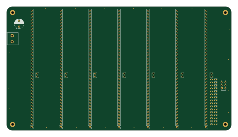
Backplane
190.5 × 105 mm49 parts2LNo license0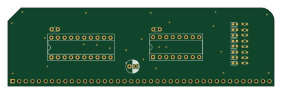
Mmu
102.5 × 30 mm22 parts2LNo license0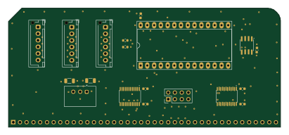
Spi
102.5 × 44.8 mm20 parts2LNo license0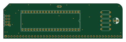
Cpu
102.5 × 30 mm10 parts2LNo license0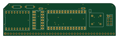
ACIA
102.5 × 30 mm10 parts2LNo license0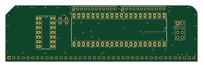
Via
102.5 × 30 mm8 parts2LNo license0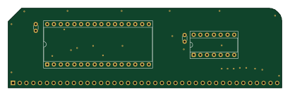
Ram
102.5 × 30 mm5 parts2LNo license0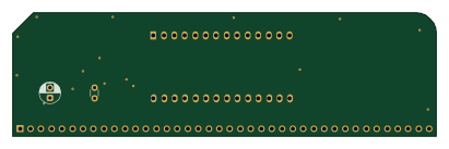
Rom
102.5 × 30 mm4 parts2LNo license0
Similar boards
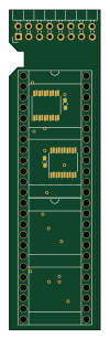
Amiga External
hoglet67
21.9 × 76.7 mm6 parts2LGPL-3.01.0k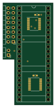
Atari pickup
26.4 × 53.9 mm7 parts2LGPL-3.01.0k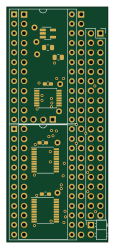
Deniseadapter
26.7 × 62.2 mm16 parts2LGPL-3.01.0k
Analog
53.9 × 23.2 mm33 parts2LGPL-3.01.0k
Rgb to hdmi
77 × 97 mm67 parts2LGPL-3.01.0k
Buffer
53.9 × 23.2 mm13 parts2LGPL-3.01.0k