
Spi

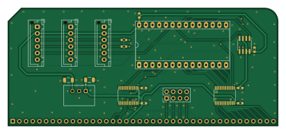
About the Spi PCB
Spi is an open source PCB design by atarola, published on GitHub. It is a 2-layer board measuring 102.5 × 44.8 mm, with 20 components from 12 distinct parts.
Other key parts include the TinyFPGA w/SPI Module, TSR1-2433E, SN74LVC8T245PWR and FM25V05-G. By type, the board carries 8 capacitors, 5 ICs, 5 connectors and 2 resistors.
It belongs with the retro computing designs in this gallery.
From the project
Code for my 6502 build
compy6502 is an early-stage 6502 homebrew computer project. The long-term goal is to build enough hardware and firmware to run Tetris on the machine.
The design follows the spirit of Ben Eater-style breadboard/modular 6502 systems for simplicity and debuggability, but uses a different memory map based on the MMU/address-decoder architecture in docs/mmu.png.
The repo currently includes KiCad hardware designs, early ROM bring-up firmware, build/write scripts, emulator test scaffolding, and architecture reference images in docs/.
Main components on the Spi
Spi bill of materials (BOM)
20 components, 12 distinct parts.
| Qty | Part | Footprint | Refs |
|---|---|---|---|
| 1 | TinyFPGA w/SPI Module | DIP-28_W15.24mm_Socket_LongPads | U1 |
| 1 | TSR1-2433E | Converter_DCDC_TRACO_TSR1-xxxxE_THT | U2 |
| 2 | SN74LVC8T245PWR | TSSOP-24_4.4x7.8mm_P0.65mm | U3, U4 |
| 1 | FM25V05-G | SOIC-8_3.9x4.9mm_P1.27mm | U5 |
| 1 | Board Connector | PinHeader_1x40_P2.54mm_Horizontal | J1 |
| 1 | IO Select | PinHeader_2x04_P2.54mm_Vertical | J3 |
| 1 | SPI 1 | JST_XH_B6B-XH-AM_1x06_P2.50mm_Vertical | J6 |
| 1 | SPI 2 | JST_XH_B6B-XH-AM_1x06_P2.50mm_Vertical | J7 |
| 1 | SPI 3 | JST_XH_B6B-XH-AM_1x06_P2.50mm_Vertical | J8 |
| 2 | 10u | C_1206_3216Metric | C1, C2 |
| 6 | 100n | C_0603_1608Metric | C3, C4, C5, C6, C7, C8 |
| 2 | 33 | R_0603_1608Metric | R1, R2 |
Spi design files
The KiCad project lives in the atarola/compy6502 repository on GitHub; these links point at the commit this page was built from.
- Layoutkicad/spi/spi.kicad_pcb
- Schematickicad/spi/spi.kicad_sch
Spi: common questions
How big is the Spi PCB?
The Spi measures 102.5 × 44.8 mm, has 2 copper layers and is 1.6 mm thick.
How many components are on the Spi?
20 components, from 12 distinct parts. The full bill of materials is listed on this page.
Where can I download the Spi design files?
From the atarola/compy6502 repository on GitHub, which has the KiCad layout and the schematic; the links under Design files point to each one.
Can I use the Spi design in my own project?
The repository has no license, so all rights stay with atarola. Use it as a reference, and ask the author before reusing the design.
More boards in compy6502
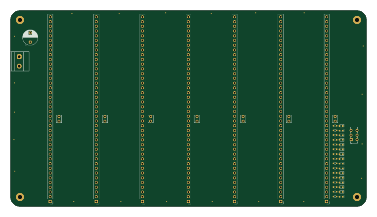
Backplane
190.5 × 105 mm49 parts2LNo license0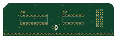
Mmu
102.5 × 30 mm22 parts2LNo license0
ACIA
102.5 × 30 mm10 parts2LNo license0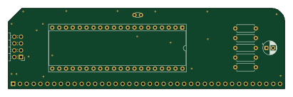
Cpu
102.5 × 30 mm10 parts2LNo license0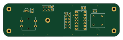
Panel
105.4 × 30.1 mm9 parts2LNo license0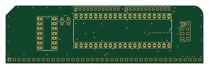
Via
102.5 × 30 mm8 parts2LNo license0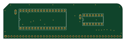
Ram
102.5 × 30 mm5 parts2LNo license0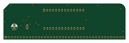
Rom
102.5 × 30 mm4 parts2LNo license0
Similar boards
Amiga External
hoglet67
21.9 × 76.7 mm6 parts2LGPL-3.01.0k
Atari pickup
26.4 × 53.9 mm7 parts2LGPL-3.01.0k
Deniseadapter
26.7 × 62.2 mm16 parts2LGPL-3.01.0k
Analog
53.9 × 23.2 mm33 parts2LGPL-3.01.0k
Rgb to hdmi
77 × 97 mm67 parts2LGPL-3.01.0k
Buffer
53.9 × 23.2 mm13 parts2LGPL-3.01.0k