
Sub


About the Sub PCB
Sub is an open source PCB design by atopile, published on GitHub under the MIT license. It is a 2-layer board, with 3 components from 1 distinct parts.
It belongs with the displays & leds designs in this gallery.
From the project
Design circuit boards with code! ✨ Get software-like design reuse 🚀, validation, version control and collaboration in hardware; starting with electronics ⚡️
Write hardware like software. atopile is a language, compiler, and toolchain for electronics—declarative .ato files, deep validation, and layout that works natively with KiCad.
- Reusable modules instead of starting from scratch every time - Capture intent with equations directly in your design - Automatic parametric picking of discrete components
The easiest way is via the editor extension—it installs and manages ato for you:
Sub bill of materials (BOM)
3 components, 1 distinct parts — part numbers from the project's BOM.
| Qty | Part | Footprint | Refs |
|---|---|---|---|
| 3 | 0402WGF1001TCE 1kΩ UNI-ROYAL(Uniroyal Elec) | R0402 | R1, R2, R3 |
Sub design files
The KiCad project lives in the atopile/atopile repository on GitHub; these links point at the commit this page was built from.
Sub: common questions
How big is the Sub PCB?
The Sub has 2 copper layers and is 1.6 mm thick.
How many components are on the Sub?
3 components, from 1 distinct parts, with part numbers taken from the project's own BOM. The full bill of materials is listed on this page.
Where can I download the Sub design files?
From the atopile/atopile repository on GitHub, which has the KiCad layout and the BOM; the links under Design files point to each one.
Can I use the Sub design in my own project?
Yes, under the terms of its MIT license, which atopile chose for the repository.
More boards in atopile

Similar boards
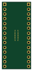
BM28B0.6-24DSBreakout
scottbez1
15.2 × 35.6 mm3 parts2LApache-2.022.2k
LevelShifterBreakout
15.2 × 20.3 mm5 parts2LApache-2.022.2k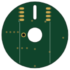
View screen
35 × 35 mm12 parts2LApache-2.022.2k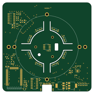
View base
81.2 × 81.2 mm81 parts2LApache-2.022.2k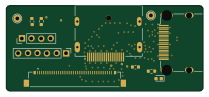
Display eval
byrantech
52.1 × 22.6 mm12 parts4LMIT4.3k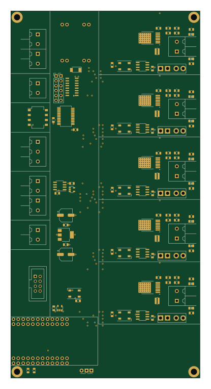
ChainlinkBase
98.4 × 190.5 mm119 parts2LApache-2.04.2k