
Micro vault dev board

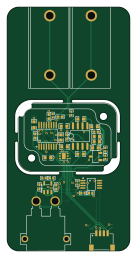
About the Micro vault dev board
Micro vault dev board is an open source PCB design by atopile, published on GitHub under the MIT license. It is a 2-layer board measuring 32.4 × 64.4 mm, with 39 components from 19 distinct parts.
Other key parts include the 24.243.2, 24.243.1, ADS1219IPWR, TLV9032DGKR and REF5050AIDR. By type, the board carries 19 resistors, 10 capacitors, 7 ICs, 1 transistor, 1 crystal and 1 connector.
It belongs with the dev boards & breakouts designs in this gallery.
From the project
Hardware-In-the-Loop (HiL ⛰️) for high-quality validation 🧪 everywhere 🚀
Hardware-in-the-Loop, or HiL (sometimes HitL), is a way to continuously validate your hardware and firmware together. By connecting actual hardware to virtual test scenarios, HiL enables thorough testing of embedded systems, control units, and firmware under realistic conditions without the risks and costs of full physical testing.
HiL testing catches integration issues early, accelerates development cycles, and ensures robust system performance before deployment. Typically the domain of the most sophisticated automotive and aerospace companies, this HiL suite is now for all 🚀.
Main components on the Micro vault dev board
Micro vault dev board bill of materials (BOM)
39 components, 19 distinct parts.
| Qty | Part | Footprint | Refs |
|---|---|---|---|
| 1 | 24.243.2 Changzhou Amass Elec | CONN-TH_24.243.2-306a6a | U1 |
| 1 | 24.243.1 Changzhou Amass Elec | CONN-TH_24.243.1_RED-2aff94 | U2 |
| 1 | ADS1219IPWR Texas Instruments | TSSOP-16_L5.0-W4.4-P0.65-LS6.4-BL-4f6acc | U5 |
| 1 | TLV9032DGKR Texas Instruments | VSSOP-8_L3.0-W3.0-P0.65-LS4.9-BL-beff67 | U6 |
| 1 | REF5050AIDR Texas Instruments | SOIC-8_L5.0-W4.0-P1.27-LS6.0-BL-294f77 | U7 |
| 1 | LDK220M-R STMicroelectronics | SOT-23-5_L3.0-W1.7-P0.95-LS2.8-BL | U8 |
| 1 | TMP117AIDRVR Texas Instruments | WSON-6_L2.0-W2.0-P0.65-TL-EP-c93430 | U9 |
| 1 | IRLML0040TRPBF Infineon Technologies | SOT-23-3_L2.9-W1.6-P1.90-LS2.8-BR-186170 | Q1 |
| 1 | SM04B-SRSS-TB(LF)(SN) JST Sales America | CONN-SMD_4P-P1.00_SM04B-SRSS-TB-LF-SN-d36980 | X1 |
| 1 | XT30PW-M30.G.Y AMASS | CONN-TH_XT30PW-M | J1 |
| 3 | CL05B104KO5NNNC 100nF ±10% 16V X7R Samsung Electro-Mechanics | C0402-b3ef17 | C1, C3, C10 |
| 3 | CL10A106KP8NNNC 10µF ±10% 10V X5R Samsung Electro-Mechanics | C0603-bd72f6 | C2, C6, C7 |
| 4 | CL05A105KA5NQNC 1µF ±10% 25V X5R Samsung Electro-Mechanics | C0402-b3ef17 | C4, C5, C8, C9 |
| 1 | 0402WGF1004TCE 1MΩ ±1% 62.5mW UNI-ROYAL(Uniroyal Elec) | R0402-56259e | R1 |
| 8 | 0603WAF150JT5E 15Ω ±1% 100mW UNI-ROYAL(Uniroyal Elec) | R0603-ebcab9 | R2, R3, R4, R5, R6, R7, R8, R9 |
| 7 | 0402WGF1002TCE 10kΩ ±1% 62.5mW UNI-ROYAL(Uniroyal Elec) | R0402-56259e | R10, R11, R14, R16, R17, R18, R19 |
| 1 | RTT021202FTH 12kΩ ±1% 62.5mW RALEC | R0402-56259e | R12 |
| 1 | RT0402BRD0788K7L 88.7kΩ ±0% 62.5mW YAGEO | R0402-56259e | R13 |
| 1 | RC0402FR-0736KL 36kΩ ±1% 62.5mW YAGEO | R0402-56259e | R15 |
Micro vault dev board design files
The KiCad project lives in the atopile/hil repository on GitHub; these links point at the commit this page was built from.
Micro vault dev board: common questions
How big is the Micro vault dev board?
The Micro vault dev board measures 32.4 × 64.4 mm, has 2 copper layers and is 1.6 mm thick.
How many components are on the Micro vault dev board?
39 components, from 19 distinct parts. The full bill of materials is listed on this page.
Where can I download the Micro vault dev board design files?
From the atopile/hil repository on GitHub, which has the KiCad layout; the links under Design files point to each one.
Can I use the Micro vault dev board design in my own project?
Yes, under the terms of its MIT license, which atopile chose for the repository.
More boards in hil

Cellsim-8ch
13 × 9 mm608 parts4LMIT29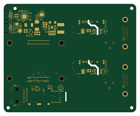
Canjay
122 × 100 mm152 parts6LMIT29
Hil core
1.5 × 9.6 mm114 parts4LMIT29
Thermistor-8ch
29.7 × 28.3 mm78 parts4LMIT29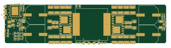
Buck boost
85.9 × 20.8 mm69 parts6LMIT29
Cell
95.1 × 8.4 mm64 parts4LMIT29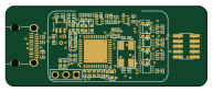 STM32
STM32Black magic probe
48.1 × 19.2 mm61 parts2LMIT29 STM32
STM32Black magic debugger
23.7 × 14.4 mm52 parts2LMIT29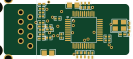
Ethernet
33.2 × 13.6 mm32 parts2LMIT29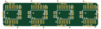
Ads1219-test
36.3 × 8.9 mm24 parts2LMIT29
Analog out
16 × 5 mm8 parts2LMIT29
Similar boards
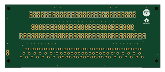
88 Pin Vag Breakout
rusefi
142 × 58 mm91 parts2LGPL-3.01.2k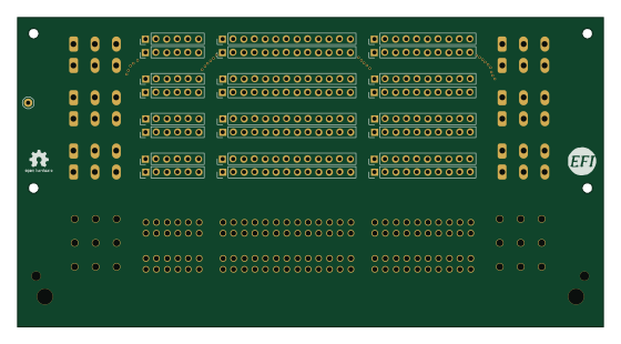
134pin 7-967288-1
139.7 × 73.7 mm38 parts2LGPL-3.01.2k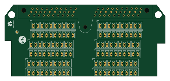
Breakout 60pin EEC-IV
139.7 × 62.2 mm15 parts2LGPL-3.01.2k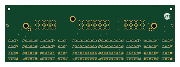
Breakout 112pin Connector
174 × 58 mm39 parts2LGPL-3.01.2k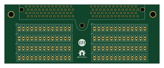
Eecv breakout
140.8 × 53.7 mm9 parts4LGPL-3.01.2k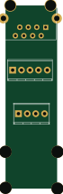
Rj45 breakout
rene-dev
15.2 × 53.8 mm3 parts2LGPL-3.0979