
Nano delay pedal

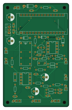
About the Nano delay pedal PCB
Nano delay pedal is an open source AVR/Arduino PCB design by barlasardic, published on GitHub under the MIT license. It is a 2-layer board measuring 55.9 × 88.9 mm, with 57 components from 33 distinct parts.
Its main chip is the Arduino_Nano_v3.x, from the AVR/Arduino family. Other key parts include the LM7805_TO220, MCP6002-I/P and 23LC1024-I/P. By type, the board carries 20 capacitors, 18 resistors, 8 connectors, 4 diodes, 3 ICs and 1 module.
It belongs with the audio designs in this gallery.
From the project
A delay pedal for electric guitars using arduino nano.
A compact guitar delay pedal prototype built around a classic Arduino Nano, with a 300 ms delay target. The schematic and two-layer PCB are complete as a first hardware draft. Firmware has not been developed, the circuit has not been built or tested, and the enclosure fit is not confirmed.
The 55.88 × 88.90 mm PCB has rounded corners and four M2.5 mounting holes. It targets a custom compact pedal enclosure. The mechanical drawing shows the proposed enclosure arrangement and an exact PCB mounting template; actual hardware clearances still need confirmation.
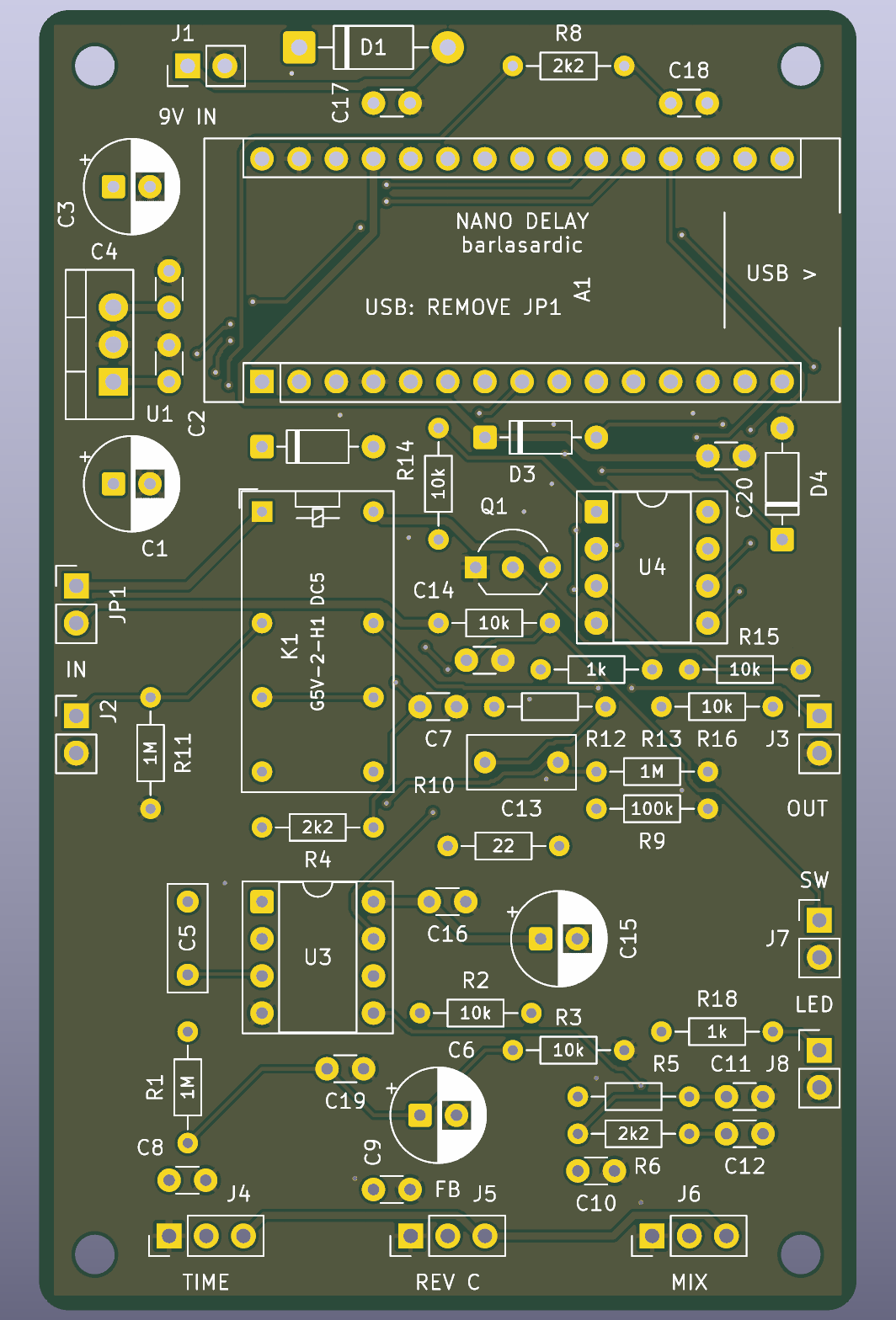
Main components on the Nano delay pedal
Nano delay pedal bill of materials (BOM)
57 components, 33 distinct parts.
| Qty | Part | Footprint | Refs |
|---|---|---|---|
| 1 | LM7805_TO220 | TO-220-3_Vertical | U1 |
| 1 | MCP6002-I/P | DIP-8_W7.62mm_Socket | U3 |
| 1 | 23LC1024-I/P | DIP-8_W7.62mm_Socket | U4 |
| 1 | Arduino_Nano_v3.x | Arduino_Nano_EdgeUSB | A1 |
| 1 | 2N3904 | TO-92_Inline_Wide | Q1 |
| 1 | 9V IN: 1=+ 2=GND | PinHeader_1x02_P2.54mm_Vertical | J1 |
| 1 | INPUT: 1=TIP 2=SLEEVE | PinHeader_1x02_P2.54mm_Vertical | J2 |
| 1 | OUTPUT: 1=TIP 2=SLEEVE | PinHeader_1x02_P2.54mm_Vertical | J3 |
| 1 | TIME B10k | PinHeader_1x03_P2.54mm_Vertical | J4 |
| 1 | FEEDBACK B10k | PinHeader_1x03_P2.54mm_Vertical | J5 |
| 1 | MIX B10k | PinHeader_1x03_P2.54mm_Vertical | J6 |
| 1 | MOMENTARY NO | PinHeader_1x02_P2.54mm_Vertical | J7 |
| 1 | LED: 1=A 2=K | PinHeader_1x02_P2.54mm_Vertical | J8 |
| 1 | POWER LINK: remove for USB | PinHeader_1x02_P2.54mm_Vertical | JP1 |
| 1 | G5V-2-H1 DC5 | Relay_DPDT_Omron_G5V-2 | K1 |
| 1 | 1N4007 | D_DO-41_SOD81_P10.16mm_Horizontal | D1 |
| 1 | 1N4148 | D_DO-35_SOD27_P7.62mm_Horizontal | D2 |
| 2 | BAT85 | D_DO-35_SOD27_P7.62mm_Horizontal | D3, D4 |
| 1 | 47u 25V | CP_Radial_D6.3mm_P2.50mm | C1 |
| 1 | 330n | C_Disc_D3.0mm_W1.6mm_P2.50mm | C2 |
Show 13 more
| Qty | Part | Footprint | Refs |
|---|---|---|---|
| 2 | 47u 16V | CP_Radial_D6.3mm_P2.50mm | C3, C6 |
| 9 | 100n | C_Disc_D3.0mm_W1.6mm_P2.50mm | C4, C8, C9, C10, C14, C16, C17, C19 +1 |
| 1 | 100n film | C_Rect_L7.2mm_W2.5mm_P5.00mm | C5 |
| 4 | 10n | C_Disc_D3.0mm_W1.6mm_P2.50mm | C7, C11, C12, C18 |
| 1 | 1u film | C_Rect_L7.2mm_W3.5mm_P5.00mm | C13 |
| 1 | 100u 16V | CP_Radial_D6.3mm_P2.50mm | C15 |
| 3 | 1M | R_Axial_DIN0204_L3.6mm_D1.6mm_P7.62mm_Horizontal | R1, R11, R13 |
| 6 | 10k | R_Axial_DIN0204_L3.6mm_D1.6mm_P7.62mm_Horizontal | R2, R3, R14, R15, R16, R17 |
| 4 | 2k2 | R_Axial_DIN0204_L3.6mm_D1.6mm_P7.62mm_Horizontal | R4, R5, R6, R8 |
| 2 | 1k | R_Axial_DIN0204_L3.6mm_D1.6mm_P7.62mm_Horizontal | R7, R18 |
| 1 | 100k | R_Axial_DIN0204_L3.6mm_D1.6mm_P7.62mm_Horizontal | R9 |
| 1 | 22 | R_Axial_DIN0204_L3.6mm_D1.6mm_P7.62mm_Horizontal | R10 |
| 1 | 100 | R_Axial_DIN0204_L3.6mm_D1.6mm_P7.62mm_Horizontal | R12 |
Nano delay pedal design files
The KiCad project lives in the barlasardic/nano-delay-pedal repository on GitHub; these links point at the commit this page was built from.
- Layoutdelay-pedal.kicad_pcb
- Schematicdelay-pedal.kicad_sch
Nano delay pedal: common questions
What microcontroller does the Nano delay pedal use?
The Nano delay pedal is built around the Arduino_Nano_v3.x, from the AVR/Arduino family.
How big is the Nano delay pedal PCB?
The Nano delay pedal measures 55.9 × 88.9 mm, has 2 copper layers and is 1.6 mm thick.
How many components are on the Nano delay pedal?
57 components, from 33 distinct parts. The full bill of materials is listed on this page.
Where can I download the Nano delay pedal design files?
From the barlasardic/nano-delay-pedal repository on GitHub, which has the KiCad layout and the schematic; the links under Design files point to each one.
Can I use the Nano delay pedal design in my own project?
Yes, under the terms of its MIT license, which barlasardic chose for the repository.
Can I test firmware for the Nano delay pedal without the hardware?
Yes. HardLabs builds a simulation of the board from its netlist and BOM, so you can run and debug AVR/Arduino firmware against it before you order a PCB.
Similar boards
 AVR/Arduino
Magspoof
samyk
35 × 29 mm11 parts2LNo license4.2k AVR/Arduino
Redox keyboard
mattdibi
162.2 × 126.5 mm77 parts2LMIT2.0k AVR/Arduino
Labrador
espotek-org
36.8 × 34.7 mm75 parts2LNo license1.2k AVR/Arduino
V4
stuartpittaway
30 × 50 mm38 parts2LCC-BY-NC-4.01.1k AVR/Arduino
ModuleV450
30 × 61.4 mm39 parts2LCC-BY-NC-4.01.1k AVR/Arduino
Discipline
coseyfannitutti
304.9 × 122.8 mm170 parts2LCC-BY-NC-4.01.0k