
Awg

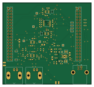
About the Awg PCB
Awg is an open source PCB design by bradencamp, published on GitHub. It is a 2-layer board measuring 78.7 × 72.6 mm, with 74 components from 24 distinct parts.
Other key parts include the LM2904, DG403 and r1283. By type, the board carries 30 resistors, 18 capacitors, 8 jumpers, 7 connectors, 6 ICs and 3 diodes.
It belongs with the test & measurement designs in this gallery.
From the project
This USB Multi-function Laboratory Instrument will be inexpensive and therefore less capable than the AD2 or ADALM 2000 while still fulfilling the requirements for most laboratory exercises in the undergraduate ECE curriculum. This new device should use a microcontroller with ana
This USB Multi-function Laboratory Instrument will be inexpensive and therefore less capable than the AD2 or ADALM 2000 while still fulfilling the requirements for most laboratory exercises in the undergraduate ECE curriculum. This new device should use a microcontroller with analog front ends for the Oscilloscope and Wave Form Generator functionality. It should function as a 2 channel Oscilloscope and Arbitrary Waveform Generator (AWG) with a Bandwidth of up to 2 MHz and a sample rate of 5 Msps, a 16 channel logic analyzer, and be controllable via USB from a PC (Windows, Mac, and Linux) as…
Main components on the Awg
Awg bill of materials (BOM)
74 components, 24 distinct parts.
| Qty | Part | Footprint | Refs |
|---|---|---|---|
| 4 | LM2904 | SOT-23-8_Handsoldering | U1, U2, U3, U4 |
| 1 | DG403 | TSSOP-16-1EP_4.4x5mm_P0.65mm | U5 |
| 1 | r1283 | DFN-12 | U6 |
| 1 | USB_B | USB_B_Lumberg_2411_02_Horizontal | J1 |
| 1 | 02x02 | 2x02 | J2 |
| 2 | BNC | BNC_Amphenol_B6252HB-NPP3G-50_Horizontal | J3, J4 |
| 1 | 2x01 | 1x02 | J5 |
| 1 | nuc303_LEFT | PinHeader_2x19_P2.54mm_Vertical | J6 |
| 1 | nuc303_RIGHT | PinHeader_2x19_P2.54mm_Vertical | J7 |
| 2 | SJ | SolderJumper-2_P1.3mm_Open_TrianglePad1.0x1.5mm | JP1, JP2 |
| 6 | JP | SolderJumper-2_P1.3mm_Bridged_RoundedPad1.0x1.5mm | JP3, JP4, JP5, JP6, JP7, JP8 |
| 2 | S14 | D_SOD-323_HandSoldering | D1, D2 |
| 1 | LM4040-5 | SOT-23 | D3 |
| 2 | 4.7u | NRH2410 | L1, L2 |
| 5 | 10u | C_0805_2012Metric_Pad1.18x1.45mm_HandSolder | C1, C2, C3, C7, C8 |
| 11 | 100n | C_0603_1608Metric_Pad1.08x0.95mm_HandSolder | C4, C9, C10, C11, C12, C13, C14, C15 +3 |
| 2 | 120p | C_0603_1608Metric_Pad1.08x0.95mm_HandSolder | C5, C6 |
| 16 | 10K | R_0603_1608Metric | R1, R2, R5, R6, R7, R9, R10, R11 +8 |
| 4 | 3K3 | R_0603_1608Metric | R3, R8, R13, R18 |
| 5 | 1K | R_0603_1608Metric | R4, R14, R27, R28, R30 |
Show 4 more
| Qty | Part | Footprint | Refs |
|---|---|---|---|
| 2 | 22 | R_0603_1608Metric | R21, R22 |
| 1 | 1K5 | R_0603_1608Metric | R23 |
| 1 | 110k | R_0603_1608Metric | R24 |
| 1 | 100k | R_0603_1608Metric | R25 |
Awg design files
The KiCad project lives in the bradencamp/ECE-Lab-USB-MultiTool repository on GitHub; these links point at the commit this page was built from.
Awg: common questions
How big is the Awg PCB?
The Awg measures 78.7 × 72.6 mm, has 2 copper layers and is 1.6 mm thick.
How many components are on the Awg?
74 components, from 24 distinct parts. The full bill of materials is listed on this page.
Where can I download the Awg design files?
From the bradencamp/ECE-Lab-USB-MultiTool repository on GitHub, which has the KiCad layout and the schematic; the links under Design files point to each one.
Can I use the Awg design in my own project?
The repository has no license, so all rights stay with bradencamp. Use it as a reference, and ask the author before reusing the design.
More boards in ECE-Lab-USB-MultiTool
Similar boards
LevelShifter
gusmanb
28.3 × 39.8 mm21 parts2LGPL-3.05.0k
StackLink
52.3 × 10.5 mm5 parts2LGPL-3.05.0k
AnalyzerBoxPCB fork
52.7 × 47.9 mm54 parts4LGPL-3.05.0k
EleLab v2 Bus100
Chrismettal
100 × 100 mm37 parts2LGPL-3.0528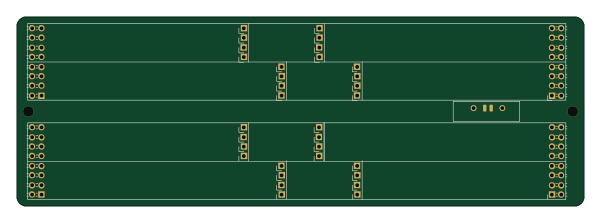
EleLab v2 Bus150
150 × 50 mm37 parts2LGPL-3.0528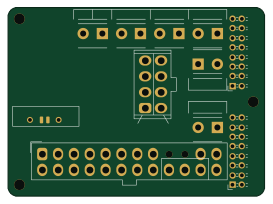
EleLab v2 PowerFeed
68 × 50 mm11 parts2LGPL-3.0528