
Dual PPU For Nintendo Famicom

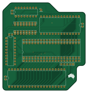
About the Dual PPU For Nintendo Famicom PCB
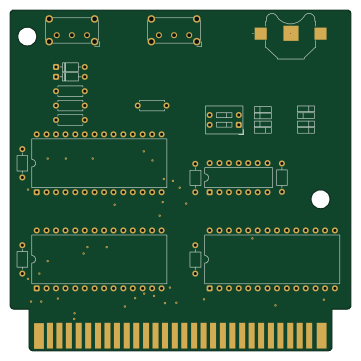
Dual PPU For Nintendo Famicom is an open source PCB design by BrettHallen, published on GitHub. It is a 2-layer board measuring 72.4 × 76.8 mm, with 14 components from 11 distinct parts.
Other key parts include the 74LS139 #2, 74LS373 #2, 74LS139 #1, 6264 VRAM#2 and RP2C02G PPU #1. By type, the board carries 6 ICs, 4 capacitors, 3 connectors and 1 resistor.
It belongs with the retro computing designs in this gallery.
From the project
Information regarding the Nintendo Family Computer
I'm informed that the schematics were originally drawn by Enri.
Also includes a Python script to patch the v3 ROM to allow 8KB of RAM and also fix some bugs.
- Disassembly - Cartridge schematics - Leaded Solder's investigation
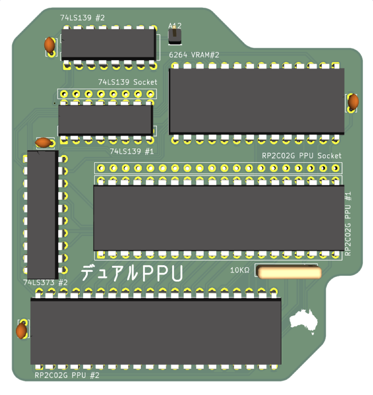
Main components on the Dual PPU For Nintendo Famicom
Dual PPU For Nintendo Famicom bill of materials (BOM)
14 components, 11 distinct parts.
| Qty | Part | Footprint | Refs |
|---|---|---|---|
| 1 | 74LS139 #2 | DIP-16_W7.62mm | U1 |
| 1 | 74LS373 #2 | DIP-20_W7.62mm | U2 |
| 1 | 74LS139 #1 | DIP-16_W7.62mm | U3 |
| 1 | 6264 VRAM#2 | DIP-28_W15.24mm | U4 |
| 1 | RP2C02G PPU #1 | DIP-40_W15.24mm | U5A1 |
| 1 | RP2C02G PPU #2 | DIP-40_W15.24mm | U5B1 |
| 1 | RP2C02G PPU Socket | DIP-40_W15.24mm | J1 |
| 1 | A12 | PinHeader_1x01_P2.54mm_Vertical | J2 |
| 1 | 74LS139 Socket | DIP-16_W7.62mm | J3 |
| 4 | 100nF | C_Disc_D3.4mm_W2.1mm_P2.50mm | C1, C2, C3, C4 |
| 1 | 10KΩ | R_Array_SIP5 | RN1 |
Dual PPU For Nintendo Famicom design files
The KiCad project lives in the BrettHallen/Nintendo-Famicom repository on GitHub; these links point at the commit this page was built from.
Dual PPU For Nintendo Famicom: common questions
How big is the Dual PPU For Nintendo Famicom PCB?
The Dual PPU For Nintendo Famicom measures 72.4 × 76.8 mm, has 2 copper layers and is 1.6 mm thick.
How many components are on the Dual PPU For Nintendo Famicom?
14 components, from 11 distinct parts. The full bill of materials is listed on this page.
Where can I download the Dual PPU For Nintendo Famicom design files?
From the BrettHallen/Nintendo-Famicom repository on GitHub, which has the KiCad layout and the schematic; the links under Design files point to each one.
Can I use the Dual PPU For Nintendo Famicom design in my own project?
The repository has no license, so all rights stay with BrettHallen. Use it as a reference, and ask the author before reusing the design.
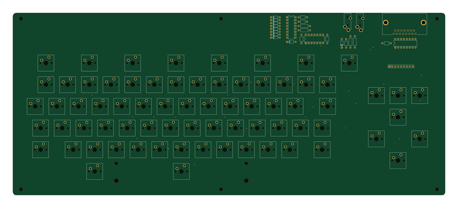
More boards in Nintendo-Famicom
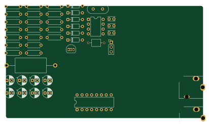
Similar boards
Expansion Card Retrofit
FrameworkComputer
24 × 27.3 mm5 parts2LCC-BY-4.01.1k
Rgb to hdmi
hoglet67
77 × 97 mm67 parts2LGPL-3.01.0k
Buffer
53.9 × 23.2 mm13 parts2LGPL-3.01.0k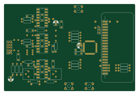
X1
121.9 × 81.3 mm51 parts2LGPL-3.01.0k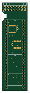
Amiga External
21.9 × 76.7 mm6 parts2LGPL-3.01.0k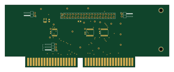
Videoslotadapter
152 × 57.6 mm13 parts2LGPL-3.01.0k