
RP2350B QFN-80 Minimal Design Example

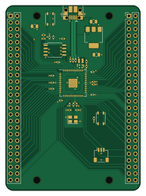
About the RP2350B QFN-80 Minimal Design Example PCB
RP2350B QFN-80 Minimal Design Example is an open source RP2040/RP2350 PCB design by Bubi2001, published on GitHub under the MIT license. It is a 2-layer board measuring 52 × 71.5 mm, with 45 components from 21 distinct parts.
Its main chip is the RP2350_80QFN, from the RP2040/RP2350 family. Other key parts include the NCP1117-3.3_SOT223 and W25Q128JVS. By type, the board carries 22 capacitors, 11 resistors, 4 ICs, 4 connectors, 2 switches and 1 crystal.
It belongs with the sensors, iot & wireless and rf & radio designs in this gallery.
From the project
OpenINS is an open-source Inertial Navigation System (INS) project that serves as a complete reference guide for designing and building your own high-performance sensor fusion platform. This repository documents the entire engineering process, from advanced RF PCB design and simulation to firmware development and physical verification.
The design focuses on the implementation of the RF design to add an active antena (via SMA connector) for the GPS module and a Meandered Inverted-F Antenna (MIFA) for the wireless communications. The firmware on the RP2354B will be implemented using its official SDK and the goal is to perform an Extended Kalman Filter to fuse data from all the sensors to get accurate inertial navigation data. The firmware on the ESP32C6 will be implemented using ESP-IDF and the goal is to communicate wirelessly the fused data.
Main components on the RP2350B QFN-80 Minimal Design Example
RP2350B QFN-80 Minimal Design Example bill of materials (BOM)
45 components, 21 distinct parts.
| Qty | Part | Footprint | Refs |
|---|---|---|---|
| 1 | RP2350_80QFN | RP2350-QFN-80-1EP_10x10_P0.4mm_EP3.4x3.4mm_ThermalVias | U1 |
| 1 | NCP1117-3.3_SOT223 | SOT-223-3_TabPin2 | U2 |
| 1 | W25Q128JVS | SOIC-8_5.23x5.23mm_P1.27mm | U3 |
| 1 | DNF | SOIC-8_5.23x5.23mm_P1.27mm | U4 |
| 1 | ABM8-272-T3 | Crystal_SMD_3225-4Pin_3.2x2.5mm | Y1 |
| 1 | USB_B_Micro | USB_Micro-B_Amphenol_10103594-0001LF_Horizontal | J1 |
| 2 | Conn_02x26_Odd_Even | PinHeader_2x26_P2.54mm_Vertical | J2, J3 |
| 1 | SM03B-SRSS-TB | JST_SH_SM03B-SRSS-TB_1x03-1MP_P1.00mm_Horizontal | J4 |
| 2 | SW_Push | SW_Push_1P1T_NO_Vertical_Wuerth_434133025816 | SW1, SW2 |
| 1 | 3.3u | L_pol_2016 | L1 |
| 3 | 10u | C_0805_2012Metric | C1, C5, C19 |
| 12 | 100n | C_0402_1005Metric | C2, C8, C11, C12, C13, C14, C15, C16 +4 |
| 2 | 15p | C_0402_1005Metric | C3, C4 |
| 2 | 4.7u | C_0402_1005Metric_small_pads | C6, C7 |
| 2 | 4.7u | C_0402_1005Metric | C9, C10 |
| 1 | DNF | C_0402_1005Metric | C22 |
| 4 | DNF | R_0402_1005Metric | R1, R9, R11, R13 |
| 3 | 1k | R_0402_1005Metric | R2, R4, R6 |
| 1 | 33 | R_0402_1005Metric | R3 |
| 2 | 27 | R_0402_1005Metric | R7, R8 |
Show 1 more
| Qty | Part | Footprint | Refs |
|---|---|---|---|
| 1 | 0 | R_0402_1005Metric | R10 |
RP2350B QFN-80 Minimal Design Example design files
The KiCad project lives in the Bubi2001/OpenINS repository on GitHub; these links point at the commit this page was built from.
RP2350B QFN-80 Minimal Design Example: common questions
What microcontroller does the RP2350B QFN-80 Minimal Design Example use?
The RP2350B QFN-80 Minimal Design Example is built around the RP2350_80QFN, from the RP2040/RP2350 family.
How big is the RP2350B QFN-80 Minimal Design Example PCB?
The RP2350B QFN-80 Minimal Design Example measures 52 × 71.5 mm, has 2 copper layers and is 1.6 mm thick.
How many components are on the RP2350B QFN-80 Minimal Design Example?
45 components, from 21 distinct parts. The full bill of materials is listed on this page.
Where can I download the RP2350B QFN-80 Minimal Design Example design files?
From the Bubi2001/OpenINS repository on GitHub, which has the KiCad layout and the schematic; the links under Design files point to each one.
Can I use the RP2350B QFN-80 Minimal Design Example design in my own project?
Yes, under the terms of its MIT license, which Bubi2001 chose for the repository.
Can I test firmware for the RP2350B QFN-80 Minimal Design Example without the hardware?
Yes. HardLabs builds a simulation of the board from its netlist and BOM, so you can run and debug RP2040/RP2350 firmware against it before you order a PCB.
More boards in OpenINS
Similar boards
 RP2040/RP2350
Open Book Abridged Edition
joeycastillo
85 × 115 mm29 parts2LCC-BY-SA-4.08.1k RP2040/RP2350
Corne
foostan
277.2 × 107.5 mm164 parts2LCC-BY-4.07.7k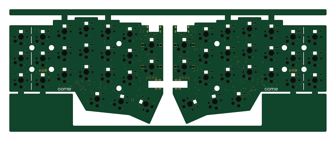 RP2040/RP2350
Corne
277.2 × 107.5 mm164 parts2LCC-BY-4.07.7k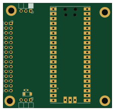 RP2040/RP2350
LogicAnalyzer
gusmanb
57 × 55.2 mm6 parts2LGPL-3.05.0k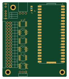 RP2040/RP2350
Jitx design
55.5 × 65 mm26 parts4LGPL-3.05.0k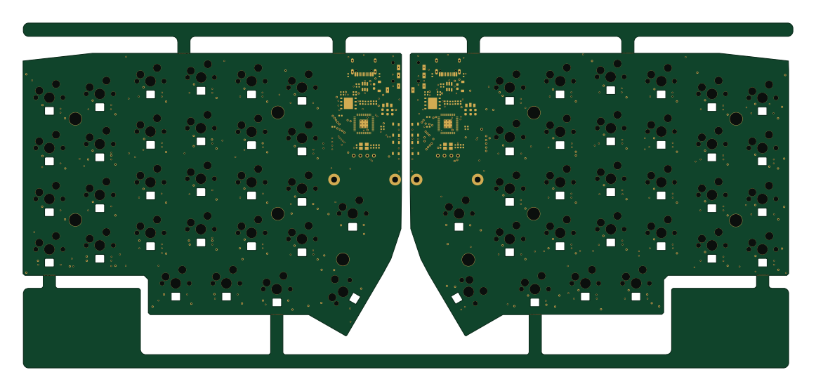 RP2040/RP2350
Pro V2
kata0510
290.1 × 130 mm270 parts2LMIT2.3k