
ActionNode

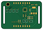
About the ActionNode PCB
ActionNode is an open source PCB design by chirambaht, published on GitHub. It is a 2-layer board measuring 43 × 30 mm, with 36 components from 19 distinct parts.
Other key parts include the MPU-6050 and AMS1117-3.3. By type, the board carries 16 connectors, 7 jumpers, 5 capacitors, 4 resistors, 2 ICs and 2 diodes.
It belongs with the sensors and iot & wireless designs in this gallery.
From the project
PCB design for the Action Trace Node.
Action Tracer differs from most systes due to its use of a 6-axes IMU and it's promise to deliver 30 frames per second with minimal latency over a Wi-Fi network.
To see more on this project, please visit the main repository: Action Tracer. ## Why a node? To monitor each articulating joint, an IMU needs to be placed near by to capture its rotation. To help this, the design houses two 20mm wide slots that allow a strap to go through it and strap it to the area it is montoring. At this stage, this design shows a wired node but future plans involve turning this node wireless. One such…
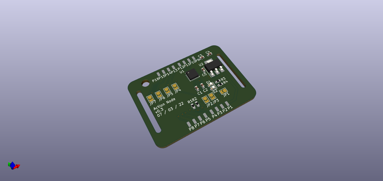
Main components on the ActionNode
ActionNode bill of materials (BOM)
36 components, 19 distinct parts — part numbers from the project's BOM.
| Qty | Part | Footprint | Refs |
|---|---|---|---|
| 1 | MPU-6050 | InvenSense_QFN-24_4x4mm_P0.5mm | U1 |
| 1 | AMS1117-3.3 | SOT-223-3_TabPin2 | U2 |
| 2 | VCC | SolderWirePad_1x01_SMD_1x2mm | P1, P9 |
| 2 | GND | SolderWirePad_1x01_SMD_1x2mm | P2, P10 |
| 2 | SCL | SolderWirePad_1x01_SMD_1x2mm | P3, P11 |
| 2 | SDA | SolderWirePad_1x01_SMD_1x2mm | P4, P12 |
| 2 | CH1 | SolderWirePad_1x01_SMD_1x2mm | P5, P13 |
| 2 | CH2 | SolderWirePad_1x01_SMD_1x2mm | P6, P14 |
| 2 | CH3 | SolderWirePad_1x01_SMD_1x2mm | P7, P15 |
| 2 | CH4 | SolderWirePad_1x01_SMD_1x2mm | P8, P16 |
| 7 | Jumper | SolderJumper-2_P1.3mm_Open_TrianglePad1.0x1.5mm | JP1, JP2, JP3, JP4, JP5, JP6, JP7 |
| 1 | C2286 Power | LED_0603_1608Metric | D1 |
| 1 | C2286 Selector | LED_0603_1608Metric | D2 |
| 1 | 10N 10n | C_0603_1608Metric | C1 |
| 2 | 0.1U 0.1u | C_0603_1608Metric | C2, C5 |
| 1 | 2.2N 2.2n | C_0603_1608Metric | C3 |
| 1 | 0.33U 0.33u | C_0603_1608Metric | C4 |
| 2 | 10K 10k | R_0603_1608Metric | R1, R2 |
| 2 | 68 | R_0603_1608Metric | R3, R4 |
ActionNode design files
The KiCad project lives in the chirambaht/ActionNode repository on GitHub; these links point at the commit this page was built from.
- LayoutActionPCB.kicad_pcb
- SchematicActionPCB.kicad_sch
- BOMjlcpcb/assembly/BOM-ActionPCB.csv
ActionNode: common questions
How big is the ActionNode PCB?
The ActionNode measures 43 × 30 mm, has 2 copper layers and is 1.6 mm thick.
How many components are on the ActionNode?
36 components, from 19 distinct parts, with part numbers taken from the project's own BOM. The full bill of materials is listed on this page.
Where can I download the ActionNode design files?
From the chirambaht/ActionNode repository on GitHub, which has the KiCad layout, the schematic and the BOM; the links under Design files point to each one.
Can I use the ActionNode design in my own project?
The repository has no license, so all rights stay with chirambaht. Use it as a reference, and ask the author before reusing the design.
Similar boards
Sensor smd
scottbez1
40 × 20 mm5 parts2LApache-2.04.2k
Sensors
StuckAtPrototype
15.2 × 9 mm14 parts4LApache-2.03.8k
EinkPDA screen
TalismanDesign
95 × 54 mm27 parts2LApache-2.02.0k
Microphone
Mentra-Community
5.5 × 6.1 mm6 parts2LMIT1.2k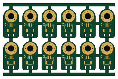
TemperaturePCB PANEL
stuartpittaway
116 × 75.5 mm178 parts2LCC-BY-NC-4.01.1k
RPi RM0 WiFi/Bluetooth Module
schlae
11.1 × 14 mm76 parts6LNo license1.0k