
ADC Buffer


About the ADC Buffer PCB
ADC Buffer is an open source PCB design by Cosys-Lab, published on GitHub under the CC-BY-SA-4.0 license. It is a 2-layer board measuring 21 × 14 mm, with 13 components from 5 distinct parts.
Other key parts include the OPA350UA/2K5. By type, the board carries 6 resistors, 3 connectors, 1 IC and 1 capacitor.
From the project
Framework for off-road rc-vehicle monitorring
- teensyboard: First version of the electrical schematic where the PCBs are subdivided based on the constrained PCB size I had to make them at home. - teensyboardv2: A V2 schematic which has an optimized schematic. This could be a good starting point to develop a new PCB. - simulationioprotection: Simulation in KiCAD to simulate the IO protection. - simulationcurrentprotection: Simulation in KiCAD to simulate the current protection. - simulationbatterystabilizer: Simulation in KiCAD to simulate the battery stabilization. - simulationadcprotection: Simulation in KiCAD to simulate the ADC…
Main components on the ADC Buffer
ADC Buffer bill of materials (BOM)
13 components, 5 distinct parts.
| Qty | Part | Footprint | Refs |
|---|---|---|---|
| 1 | OPA350UA/2K5 OPA350UA_2K5 | SOIC127P600X175-8N | IC1 |
| 3 | Conn_01x02 | PinHeader_1x02_P2.54mm_Vertical | J4, J5, J6 |
| 2 | R | TC33X2503E | RV1, RV2 |
| 1 | 10µ | C_0805_2012Metric_Pad1.18x1.45mm_HandSolder | C1 |
| 6 | R | R_0805_2012Metric_Pad1.20x1.40mm_HandSolder | R1, R2, R3, R4, R5, R6 |
ADC Buffer design files
The KiCad project lives in the Cosys-Lab/TruggySense repository on GitHub; these links point at the commit this page was built from.
ADC Buffer: common questions
How big is the ADC Buffer PCB?
The ADC Buffer measures 21 × 14 mm, has 2 copper layers and is 1.6 mm thick.
How many components are on the ADC Buffer?
13 components, from 5 distinct parts. The full bill of materials is listed on this page.
Where can I download the ADC Buffer design files?
From the Cosys-Lab/TruggySense repository on GitHub, which has the KiCad layout and the schematic; the links under Design files point to each one.
Can I use the ADC Buffer design in my own project?
Yes, under the terms of its CC-BY-SA-4.0 license, which Cosys-Lab chose for the repository.
More boards in TruggySense
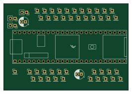 NXP
NXPTeensy boardV 1
66.5 × 46 mm590 parts2LCC-BY-SA-4.01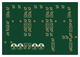
Teensy board 07 adc buffer
66.5 × 46 mm126 parts2LCC-BY-SA-4.01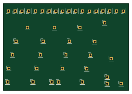
Teensy board 10 prot esd 2
66.5 × 46 mm97 parts2LCC-BY-SA-4.01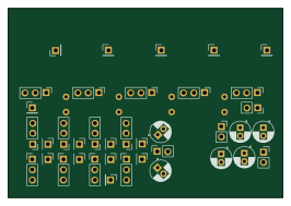
Teensy board 01 encoder prot out
66.5 × 46 mm89 parts2LCC-BY-SA-4.01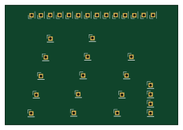
Teensy board 11 prot esd 3
66.5 × 46 mm74 parts2LCC-BY-SA-4.01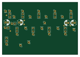
Teensy board 05 level conv
66.5 × 46 mm62 parts2LCC-BY-SA-4.01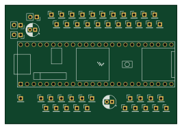 NXP
NXPTeensy board 06 main board
66.5 × 46 mm56 parts2LCC-BY-SA-4.01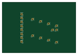
Teensy board 09 prot esd 1
66.5 × 46 mm42 parts2LCC-BY-SA-4.01
Teensy board 02 temperature
9.5 × 13.5 mm30 parts2LCC-BY-SA-4.01
Teensy board 03 LED
18.8 × 17 mm14 parts2LCC-BY-SA-4.01
Out Protection
17.4 × 13.4 mm8 parts2LCC-BY-SA-4.01