
FPGA-SCSI

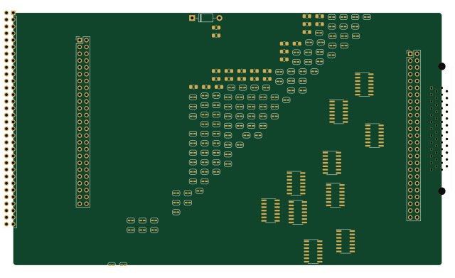
About the FPGA-SCSI PCB
FPGA-SCSI is an open source PCB design by DaveRichmond, published on GitHub under the Custom license license. It is a 2-layer board measuring 159.6 × 94 mm, with 143 components from 9 distinct parts.
Other key parts include the 74LVC125. By type, the board carries 104 jumpers, 24 resistors, 10 ICs, 4 connectors and 1 diode.
It belongs with the dev boards & breakouts designs in this gallery.
From the project
Just a bunch of PCBs I've designed for various prototyping or experimentation purposes. Mostly breakouts or adapters. CC-BY-3.0-AU
Main components on the FPGA-SCSI
FPGA-SCSI bill of materials (BOM)
143 components, 9 distinct parts.
| Qty | Part | Footprint | Refs |
|---|---|---|---|
| 10 | 74LVC125 | SOIC-14_3.9x8.7mm_P1.27mm | U1, U2, U3, U4, U5, U6, U7, U8 +2 |
| 2 | Conn_02x25_Odd_Even | PinHeader_2x25_P2.54mm_Vertical | J1, J4 |
| 1 | Conn_02x25_Top_Bottom | Amplite .050 2x25 | J2 |
| 1 | Conn_02x32_Odd_Even | PinSocket_2x32_P2.54mm_Vertical | J3 |
| 96 | Jumper_NC_Small | SolderJumper-2_P1.3mm_Bridged_RoundedPad1.0x1.5mm | JP1, JP2, JP3, JP4, JP5, JP6, JP7, JP8 +88 |
| 8 | Jumper_2_Bridged | SolderJumper-2_P1.3mm_Bridged_RoundedPad1.0x1.5mm | JP26, JP27, JP28, JP47, JP66, JP67, JP68, JP69 |
| 1 | 1N4002 | D_DO-41_SOD81_P10.16mm_Horizontal | D1 |
| 6 | R | R_0805_2012Metric_Pad1.20x1.40mm_HandSolder | R1, R2, R3, R4, R5, R6 |
| 18 | R_Small | R_0805_2012Metric_Pad1.20x1.40mm_HandSolder | R7, R8, R9, R10, R11, R12, R13, R14 +10 |
FPGA-SCSI design files
The KiCad project lives in the DaveRichmond/PCBs repository on GitHub; these links point at the commit this page was built from.
- LayoutFPGA-SCSI/FPGA-SCSI.kicad_pcb
- SchematicFPGA-SCSI/FPGA-SCSI.kicad_sch
FPGA-SCSI: common questions
How big is the FPGA-SCSI PCB?
The FPGA-SCSI measures 159.6 × 94 mm, has 2 copper layers and is 1.6 mm thick.
How many components are on the FPGA-SCSI?
143 components, from 9 distinct parts. The full bill of materials is listed on this page.
Where can I download the FPGA-SCSI design files?
From the DaveRichmond/PCBs repository on GitHub, which has the KiCad layout and the schematic; the links under Design files point to each one.
Can I use the FPGA-SCSI design in my own project?
It is published under Custom license, which limits how it may be reused; read the license before building on it.
More boards in PCBs
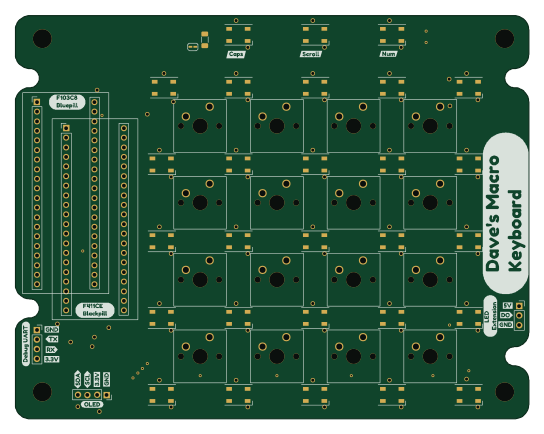
MiniKeyboard
135.9 × 106.7 mm96 parts2LCustom license0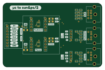
Sun-KBD-Interface
88.9 × 57.2 mm40 parts2LCustom license0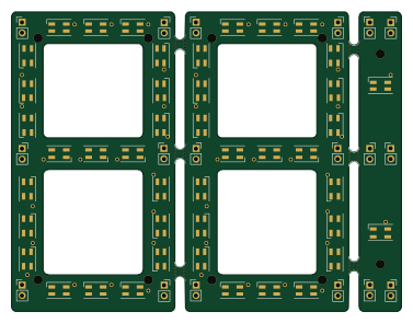
Panel
94.1 × 72.4 mm36 parts2LCustom license0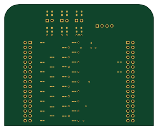
Gotek-PS2
77.2 × 63 mm18 parts2LCustom license0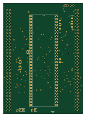
M68K-Nucleo
71.1 × 97.8 mm18 parts2LCustom license0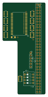
Qmtech sram
39 × 82.6 mm14 parts2LCustom license0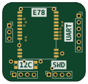
E78-breakout
31.8 × 30.5 mm10 parts2LCustom license0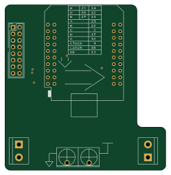 ESP32
ESP32ESP32-D1Mini-HUB75
62 × 63.8 mm5 parts2LCustom license0
Similar boards
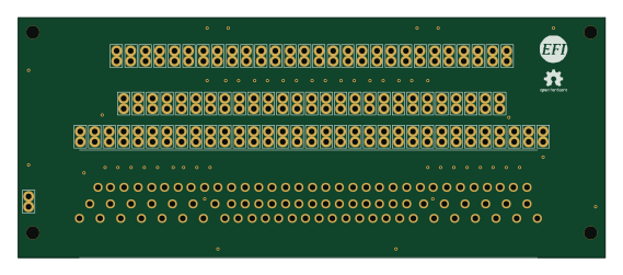
88 Pin Vag Breakout
rusefi
142 × 58 mm91 parts2LGPL-3.01.2k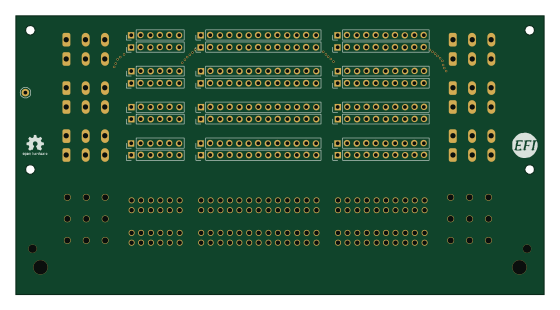
134pin 7-967288-1
139.7 × 73.7 mm38 parts2LGPL-3.01.2k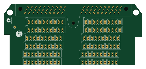
Breakout 60pin EEC-IV
139.7 × 62.2 mm15 parts2LGPL-3.01.2k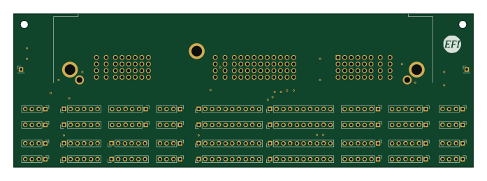
Breakout 112pin Connector
174 × 58 mm39 parts2LGPL-3.01.2k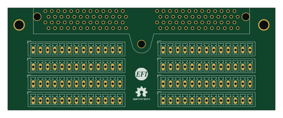
Eecv breakout
140.8 × 53.7 mm9 parts4LGPL-3.01.2k
Rj45 breakout
rene-dev
15.2 × 53.8 mm3 parts2LGPL-3.0979