
AVRISP breakout


About the AVRISP breakout
AVRISP breakout is an open source PCB design by dbuchwald, published on GitHub under the MIT license. It is a 2-layer board measuring 17.8 × 17.8 mm, with 3 components from 3 distinct parts.
It belongs with the dev boards & breakouts designs in this gallery.
From the project
Simple designs in KiCAD that do not require separate projects
AVRISP breakout bill of materials (BOM)
3 components, 3 distinct parts — part numbers from the project's BOM.
| Qty | Part | Footprint | Refs |
|---|---|---|---|
| 1 | AVRISP | PinHeader_2x03_P2.54mm_Vertical | J1 |
| 1 | Left | PinHeader_1x03_P2.54mm_Vertical | J2 |
| 1 | Right | PinHeader_1x03_P2.54mm_Vertical | J3 |
AVRISP breakout design files
The KiCad project lives in the dbuchwald/kicad-simple repository on GitHub; these links point at the commit this page was built from.
AVRISP breakout: common questions
How big is the AVRISP breakout?
The AVRISP breakout measures 17.8 × 17.8 mm, has 2 copper layers and is 1.6 mm thick.
How many components are on the AVRISP breakout?
3 components, from 3 distinct parts, with part numbers taken from the project's own BOM. The full bill of materials is listed on this page.
Where can I download the AVRISP breakout design files?
From the dbuchwald/kicad-simple repository on GitHub, which has the KiCad layout and the BOM; the links under Design files point to each one.
Can I use the AVRISP breakout design in my own project?
Yes, under the terms of its MIT license, which dbuchwald chose for the repository.
More boards in kicad-simple
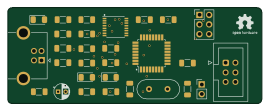 AVR/Arduino
UPDI programmer
67.3 × 25.4 mm29 parts2LMIT10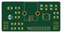
USB power serial breakout
53.3 × 26.7 mm20 parts2LMIT10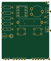
SoftPower breakout
44.5 × 53.3 mm17 parts2LMIT10
MicroSD breakout
24.1 × 22.9 mm4 parts2LMIT10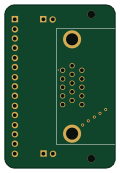
VGA breakout
29.2 × 43.2 mm4 parts2LMIT10
AVRISP10 breakout
17.8 × 17.8 mm3 parts2LMIT10
Similar boards
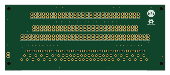
88 Pin Vag Breakout
rusefi
142 × 58 mm91 parts2LGPL-3.01.2k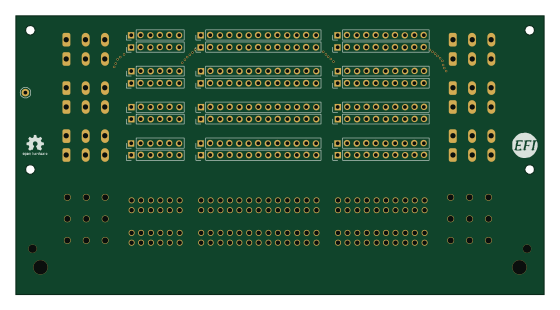
134pin 7-967288-1
139.7 × 73.7 mm38 parts2LGPL-3.01.2k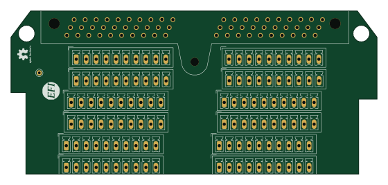
Breakout 60pin EEC-IV
139.7 × 62.2 mm15 parts2LGPL-3.01.2k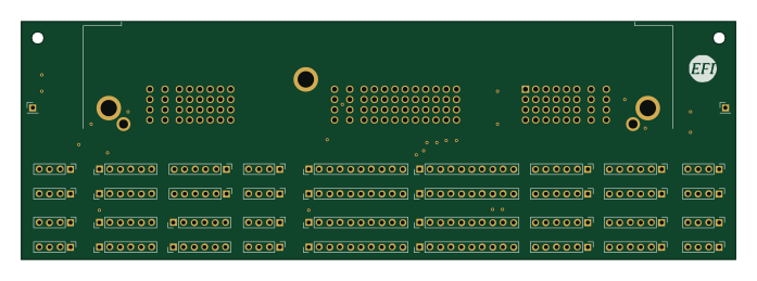
Breakout 112pin Connector
174 × 58 mm39 parts2LGPL-3.01.2k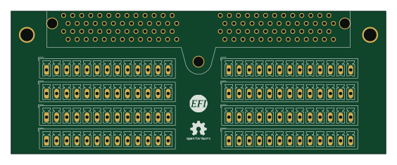
Eecv breakout
140.8 × 53.7 mm9 parts4LGPL-3.01.2k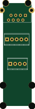
Rj45 breakout
rene-dev
15.2 × 53.8 mm3 parts2LGPL-3.0979