
SplitFlap Display Module Backplane V1.1

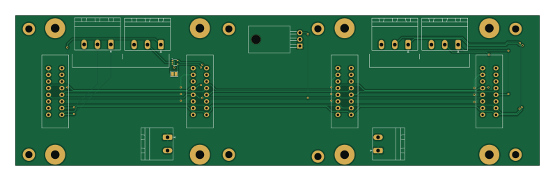
About the SplitFlap Display Module Backplane V1.1
SplitFlap Display Module Backplane V1.1 is an open source PCB design by dennis9819, published on GitHub under the AGPL-3.0 license. It is a 2-layer board measuring 199 × 57 mm, with 13 components from 6 distinct parts.
Other key parts include the L7805 and 74AHCT1G125. By type, the board carries 6 connectors, 2 ICs and 1 jumper.
It belongs with the displays & leds designs in this gallery.
From the project
Sourcecode and Schematics for the controller of my split-flap display
Welcome to split-flap-controller, the firmware + hardware design for driving a modular, scalable split-flap display system.
Development of this project began in 2024 with the goal of creating a robust, DIY split-flap display that anyone can build and customize themselves. Inspired by the iconic Frankfurt Airport display, this project aims to recreate the nostalgic mechanical aesthetic and characteristic flipping sound that made those displays so memorable.

Main components on the SplitFlap Display Module Backplane V1.1
SplitFlap Display Module Backplane V1.1 bill of materials (BOM)
13 components, 6 distinct parts.
| Qty | Part | Footprint | Refs |
|---|---|---|---|
| 1 | L7805 | TO-220-3_Horizontal_TabDown | U1 |
| 1 | 74AHCT1G125 | SOT-353_SC-70-5 | U2 |
| 2 | Conn_01x02 | PhoenixContact_MSTBA_2,5_2-G-5,08_1x02_P5.08mm_Horizontal | J1, J2 |
| 4 | Conn_01x03 | PhoenixContact_MSTBA_2,5_3-G-5,08_1x03_P5.08mm_Horizontal | J5, J6, J7, J8 |
| 4 | 2x08 Edge Connector | Card-Socket Flap Module | JM1, JM2, JM3, JM4 |
| 1 | Jumper_2_Open | SolderJumper-2_P1.3mm_Open_Pad1.0x1.5mm | JP1 |
SplitFlap Display Module Backplane V1.1 design files
The KiCad project lives in the dennis9819/split-flap-controller repository on GitHub; these links point at the commit this page was built from.
SplitFlap Display Module Backplane V1.1: common questions
How big is the SplitFlap Display Module Backplane V1.1?
The SplitFlap Display Module Backplane V1.1 measures 199 × 57 mm, has 2 copper layers and is 1.6 mm thick.
How many components are on the SplitFlap Display Module Backplane V1.1?
13 components, from 6 distinct parts. The full bill of materials is listed on this page.
Where can I download the SplitFlap Display Module Backplane V1.1 design files?
From the dennis9819/split-flap-controller repository on GitHub, which has the KiCad layout and the schematic; the links under Design files point to each one.
Can I use the SplitFlap Display Module Backplane V1.1 design in my own project?
Yes, under the terms of its AGPL-3.0 license, which dennis9819 chose for the repository.
More boards in split-flap-controller
Similar boards
BM28B0.6-24DSBreakout
scottbez1
15.2 × 35.6 mm3 parts2LApache-2.022.2k
LevelShifterBreakout
15.2 × 20.3 mm5 parts2LApache-2.022.2k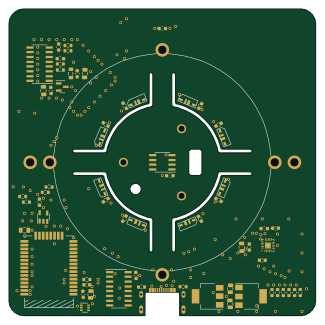
View base
81.2 × 81.2 mm81 parts2LApache-2.022.2k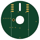
View screen
35 × 35 mm12 parts2LApache-2.022.2k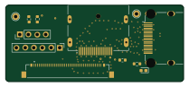
Display eval
byrantech
52.1 × 22.6 mm12 parts4LMIT4.3k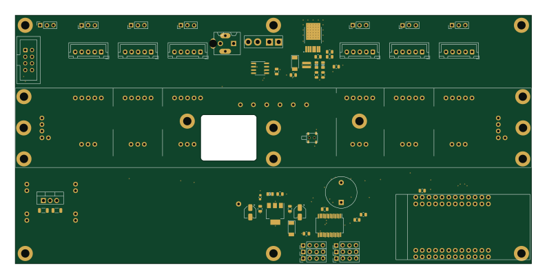
ChainlinkDriverTester
198.1 × 95.3 mm123 parts2LApache-2.04.2k