
Ec scan module


About the Ec scan module
Ec scan module is an open source PCB design by Diwamoto, published on GitHub. It is a 2-layer board measuring 16.3 × 21.4 mm, with 17 components from 8 distinct parts.
Other key parts include the TLV9061IDBVR and 74HC4051. By type, the board carries 9 resistors, 3 capacitors, 2 ICs, 2 connectors and 1 jumper.
From the project
ae_nrf52840を使って静電容量が検知できるかどうかを検証する。 100x100に入れてpcbaの費用以外を安くする。
Main components on the Ec scan module
Ec scan module bill of materials (BOM)
17 components, 8 distinct parts.
| Qty | Part | Footprint | Refs |
|---|---|---|---|
| 1 | TLV9061IDBVR | SOT-23-5 | U2 |
| 1 | 74HC4051 | TSSOP-16_4.4x5mm_P0.65mm | U3 |
| 2 | Conn_01x08 | PinHeader_1x08_P2.54mm_Vertical | J2, J3 |
| 1 | Jumper_2_Open | R_0201_0603Metric_Pad0.64x0.40mm_HandSolder | JP1 |
| 2 | 100n | C_0402_1005Metric | C1, C3 |
| 1 | 220p | C_0402_1005Metric | C2 |
| 8 | 100k | R_0402_1005Metric | R1, R2, R3, R4, R5, R6, R7, R8 |
| 1 | 1k | R_0402_1005Metric | R9 |
Ec scan module design files
The KiCad project lives in the Diwamoto/sage60 repository on GitHub; these links point at the commit this page was built from.
Ec scan module: common questions
How big is the Ec scan module?
The Ec scan module measures 16.3 × 21.4 mm, has 2 copper layers and is 1.6 mm thick.
How many components are on the Ec scan module?
17 components, from 8 distinct parts. The full bill of materials is listed on this page.
Where can I download the Ec scan module design files?
From the Diwamoto/sage60 repository on GitHub, which has the KiCad layout and the schematic; the links under Design files point to each one.
Can I use the Ec scan module design in my own project?
The repository has no license, so all rights stay with Diwamoto. Use it as a reference, and ask the author before reusing the design.
More boards in sage60
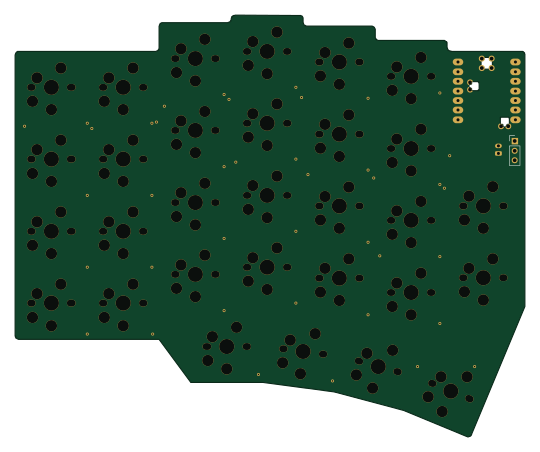 Nordic nRF
Mx
134.9 × 111.5 mm63 parts2LNo license1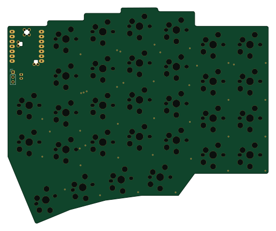 Nordic nRF
Mx right
134.9 × 111.5 mm63 parts2LNo license1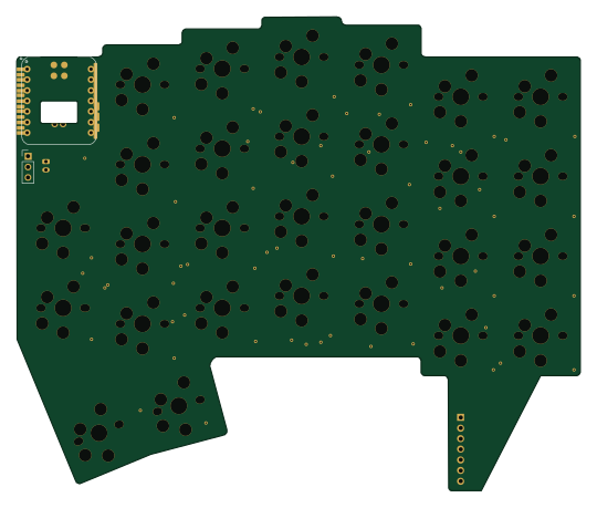 Nordic nRF
Mx right tb
134.9 × 113.3 mm60 parts2LNo license1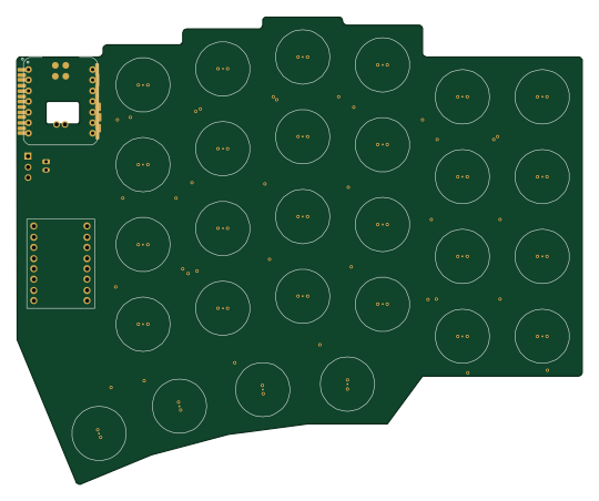 Nordic nRF
Ec right
134.9 × 111.5 mm31 parts2LNo license1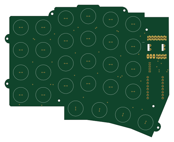 Nordic nRF
Ec
139.2 × 111.9 mm30 parts2LNo license1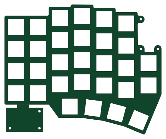
Mx plate
134.9 × 111.5 mm30 parts2LNo license1