
Ec

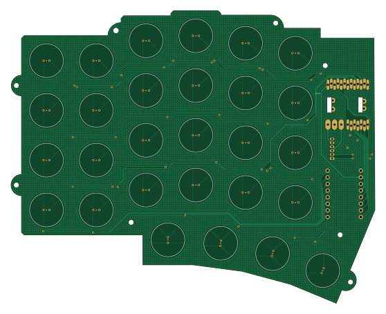
About the Ec PCB
Ec is an open source Nordic nRF PCB design by Diwamoto, published on GitHub. It is a 2-layer board measuring 139.2 × 111.9 mm, with 30 components from 3 distinct parts.
Its main chip is the XIAO_nRF52840_plus_mki, from the Nordic nRF family. By type, the board carries 28 switches, 1 IC and 1 connector.
From the project
ae_nrf52840を使って静電容量が検知できるかどうかを検証する。 100x100に入れてpcbaの費用以外を安くする。
Ec bill of materials (BOM)
30 components, 3 distinct parts.
| Qty | Part | Footprint | Refs |
|---|---|---|---|
| 1 | ~ | XIAO_nRF52840_plus_mki | U3 |
| 1 | Conn_01x06_Socket | JST_ZH_B6B-ZR_1x06_P1.50mm_Vertical | J3 |
| 28 | EC_SW | ecs_pad_1U_no_ring | SW0, SW1, SW2, SW3, SW4, SW5, SW6, SW7 +20 |
Ec design files
The KiCad project lives in the Diwamoto/sage60 repository on GitHub; these links point at the commit this page was built from.
- Layoutpcb/ec_plate/ec.kicad_pcb
- Schematicpcb/ec_plate/ec.kicad_sch
Ec: common questions
What microcontroller does the Ec use?
The Ec is built around the XIAO_nRF52840_plus_mki, from the Nordic nRF family.
How big is the Ec PCB?
The Ec measures 139.2 × 111.9 mm, has 2 copper layers and is 1.6 mm thick.
How many components are on the Ec?
30 components, from 3 distinct parts. The full bill of materials is listed on this page.
Where can I download the Ec design files?
From the Diwamoto/sage60 repository on GitHub, which has the KiCad layout and the schematic; the links under Design files point to each one.
Can I use the Ec design in my own project?
The repository has no license, so all rights stay with Diwamoto. Use it as a reference, and ask the author before reusing the design.
Can I test firmware for the Ec without the hardware?
Yes. HardLabs builds a simulation of the board from its netlist and BOM, so you can run and debug Nordic nRF firmware against it before you order a PCB.
More boards in sage60
 Nordic nRF
Mx
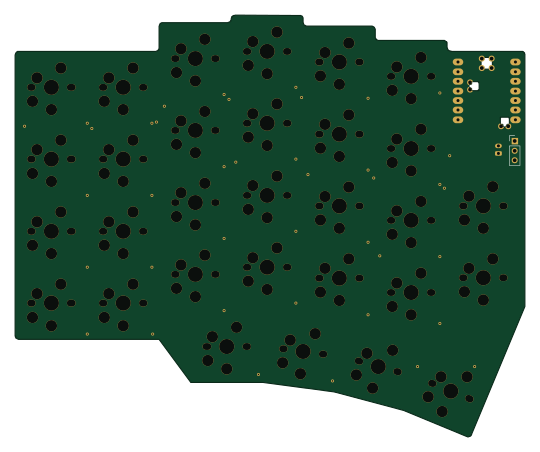
134.9 × 111.5 mm63 parts2LNo license1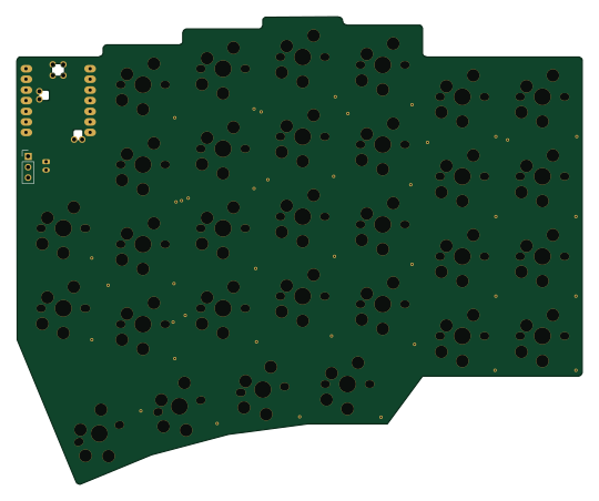 Nordic nRF
Mx right
134.9 × 111.5 mm63 parts2LNo license1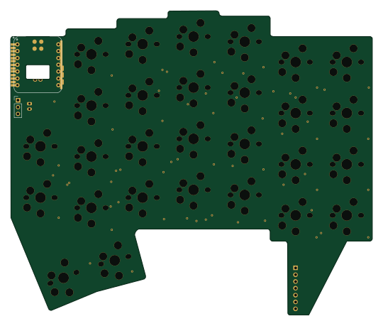 Nordic nRF
Mx right tb
134.9 × 113.3 mm60 parts2LNo license1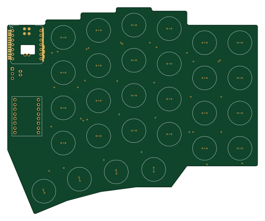 Nordic nRF
Ec right
134.9 × 111.5 mm31 parts2LNo license1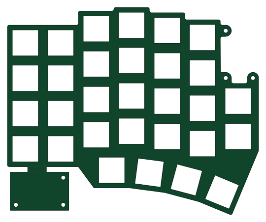
Mx plate
134.9 × 111.5 mm30 parts2LNo license1
Ec scan module
16.3 × 21.4 mm17 parts2LNo license1
Similar boards
 Nordic nRF
Keyboard
byrantech
262.5 × 109.6 mm206 parts2LMIT4.3k Nordic nRF
TOTEM
GEIGEIGEIST
258.8 × 94.4 mm85 parts2LCERN-OHL-P-2.02.0k Nordic nRF
Pixl.js
solosky
40 × 23 mm45 parts4LGPL-2.01.4k Nordic nRF
Board hl15-latest
dennisss
61 × 37 mm14 parts2LApache-2.0381 Nordic nRF
Management
101 × 31.5 mm50 parts2LApache-2.0381 Nordic nRF
Board
363 × 128 mm420 parts4LApache-2.0381