
Split flap

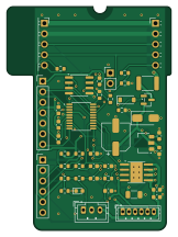
About the Split flap PCB
Split flap is an open source STM32 PCB design by DrewFerg11, published on GitHub under the CC-BY-NC-4.0 license. It is a 2-layer board measuring 39.6 × 54 mm, with 45 components from 31 distinct parts.
Its main chip is the STM32G031F8P6, from the STM32 family. Other key parts include the HT7533-1, GM3085E and DRV8870DDAR. By type, the board carries 15 resistors, 14 capacitors, 6 connectors, 4 ICs, 2 diodes and 1 transistor.
It belongs with the displays & leds designs in this gallery.
From the project
3D-printable split-flap display with custom electronics, firmware, applications, and interactive demos
Status (2026-10-27): board #1 brought up (power, SWD flash, LED, hall, encoder, motor drive all pass; see design/DESIGN-1.md section 14 and firmware/bringup). Next: other 9 boards, ISEN, RS-485 + enumeration firmware.
Status (2026-10-19): ordered. ERC 0, DRC 0 errors / 0 unconnected; the files in fab/ are what was ordered.
Ordered 2026-10-19: JLCPCB, 10 boards, Economic PCBA top side (green, 1.6 mm, HASL), est. ship 2026-10-23; C1 hand-solder caps from LCSC (20× C3151830, separate shipment).
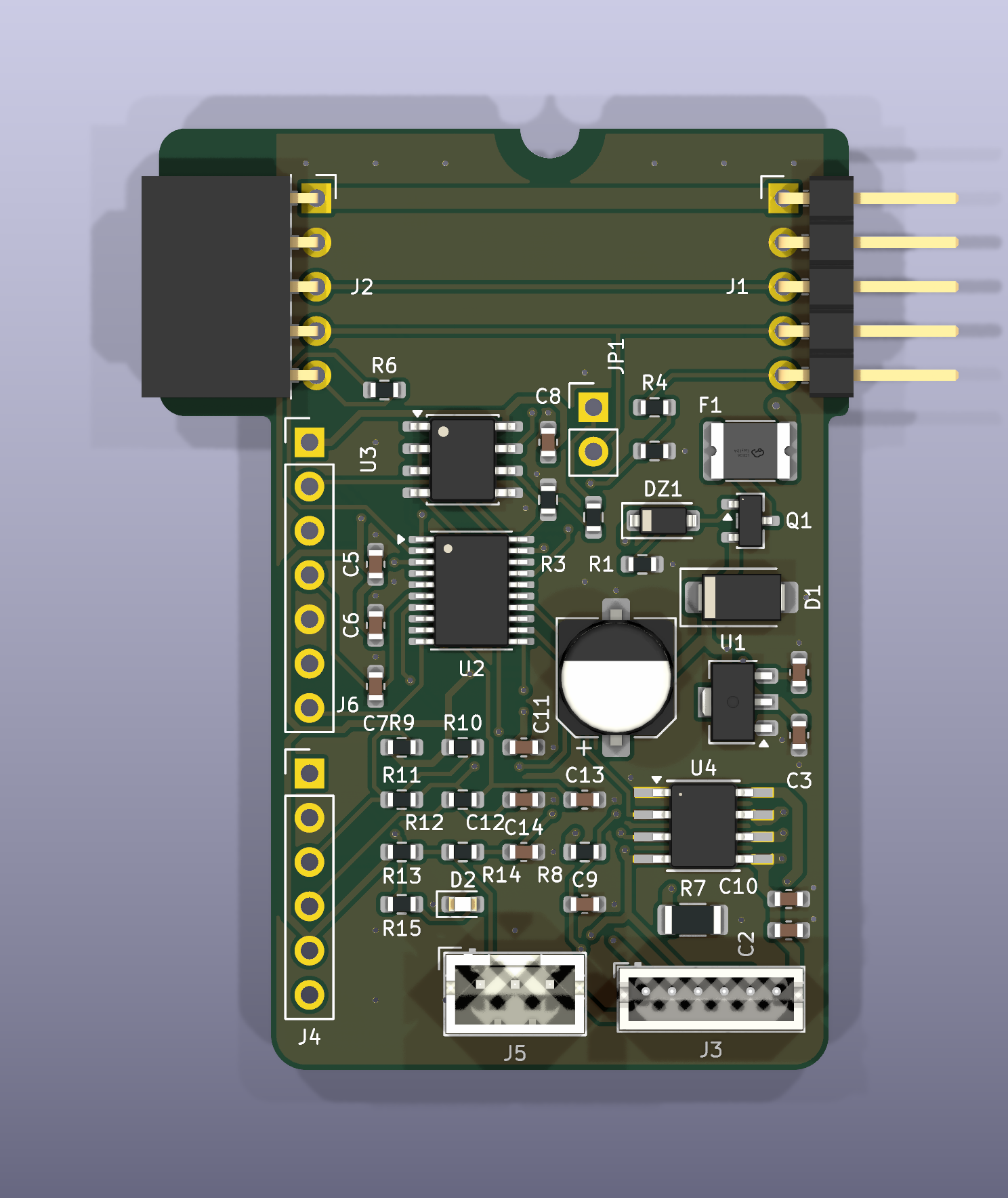
Main components on the Split flap
Split flap bill of materials (BOM)
45 components, 31 distinct parts — part numbers from the project's BOM.
| Qty | Part | Footprint | Refs |
|---|---|---|---|
| 1 | HT7533-1 | SOT-89-3 | U1 |
| 1 | STM32G031F8P6 | TSSOP-20_4.4x6.5mm_P0.65mm | U2 |
| 1 | GM3085E | SOIC-8_3.9x4.9mm_P1.27mm | U3 |
| 1 | DRV8870DDAR | Texas_HTSOP-8-1EP_3.9x4.9mm_P1.27mm_EP2.95x4.9mm_Mask2.4x3.1mm_ThermalVias | U4 |
| 1 | AO3401A | SOT-23 | Q1 |
| 1 | C492413 CHAIN_IN 5p R/A header | PinHeader_1x05_P2.54mm_Horizontal | J1 |
| 1 | C2897387 CHAIN_OUT 5p R/A socket | PinSocket_1x05_P2.54mm_Horizontal | J2 |
| 1 | C157984 MOTOR ZH1.5 6p | JST_ZH_B6B-ZR_1x06_P1.50mm_Vertical | J3 |
| 1 | MOTOR pads (DNP) | PinHeader_1x06_P2.54mm_Vertical | J4 |
| 1 | C2320 HALL PH2.0 3p | JST_PH_B3B-PH-K_1x03_P2.00mm_Vertical | J5 |
| 1 | SWD + UART pads (DNP) | PinHeader_1x07_P2.54mm_Vertical | J6 |
| 1 | C107591 MM1Z10 10V | D_SOD-123 | DZ1 |
| 1 | C7433877 2A hold 33V | Fuse_1812_4532Metric | F1 |
| 1 | JP_TERM bench only | PinHeader_1x02_P2.54mm_Vertical | JP1 |
| 1 | SMAJ18A | D_SMA | D1 |
| 1 | C2286 LED red | LED_0603_1608Metric | D2 |
| 1 | 100u 35V | CP_Elec_6.3x5.4 | C1 |
| 1 | 100N 100n 50V (VM) | C_0603_1608Metric | C2 |
| 1 | 1u 50V | C_0603_1608Metric | C3 |
| 1 | 10U 10u | C_0603_1608Metric | C4 |
Show 11 more
| Qty | Part | Footprint | Refs |
|---|---|---|---|
| 5 | 100N 100n | C_0603_1608Metric | C5, C7, C8, C9, C11 |
| 1 | 1u | C_0603_1608Metric | C6 |
| 1 | 100N 100n 50V | C_0603_1608Metric | C10 |
| 3 | 1n | C_0603_1608Metric | C12, C13, C14 |
| 2 | 100K 100k | R_0603_1608Metric | R1, R2 |
| 1 | 120R | R_0603_1608Metric | R3 |
| 4 | 1k | R_0603_1608Metric | R4, R6, R8, R15 |
| 4 | 10K 10k | R_0603_1608Metric | R5, R9, R10, R13 |
| 1 | C858786 0.33R 1% 0.5W | R_1206_3216Metric | R7 |
| 2 | 100R | R_0603_1608Metric | R11, R12 |
| 1 | 4.7K 4.7k | R_0603_1608Metric | R14 |
Split flap design files
The KiCad project lives in the DrewFerg11/split-flap repository on GitHub; these links point at the commit this page was built from.
Split flap: common questions
What microcontroller does the Split flap use?
The Split flap is built around the STM32G031F8P6, from the STM32 family.
How big is the Split flap PCB?
The Split flap measures 39.6 × 54 mm, has 2 copper layers and is 1.6 mm thick.
How many components are on the Split flap?
45 components, from 31 distinct parts, with part numbers taken from the project's own BOM. The full bill of materials is listed on this page.
Where can I download the Split flap design files?
From the DrewFerg11/split-flap repository on GitHub, which has the KiCad layout, the schematic and the BOM; the links under Design files point to each one.
Can I use the Split flap design in my own project?
It is published under CC-BY-NC-4.0, which limits how it may be reused; read the license before building on it.
Can I test firmware for the Split flap without the hardware?
Yes. HardLabs builds a simulation of the board from its netlist and BOM, so you can run and debug STM32 firmware against it before you order a PCB.
Similar boards
 STM32
LumenPnP Motherboard
opulo-inc
149 × 95 mm296 parts4LCC-BY-SA-4.03.7k STM32
Type g
google
169 × 30 mm24 parts2LApache-2.02.9k STM32
Main panel
234 × 84 mm26 parts4LApache-2.02.9k STM32
Base
52.3 × 52.3 mm36 parts2LApache-2.02.9k STM32
Type a
150 × 30 mm14 parts2LApache-2.02.9k STM32
Type c
188 × 30 mm17 parts2LApache-2.02.9k