
E1-phone mainboard routed

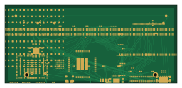
About the E1-phone mainboard routed PCB
E1-phone mainboard routed is an open source PCB design by elizaOS, published on GitHub. It is a 2-layer board measuring 64 × 29 mm, with 17 components from 17 distinct parts.
It belongs with the power & battery and iot & wireless designs in this gallery.
From the project
Hardware, silicon & embodiment research for elizaOS
Date: 2026-05-20 Status: concept_only. Non-release schematic scaffold and concept PCB exist. No reviewed schematic, routed PCB, ERC/DRC-clean layout, or fabrication output exists.
Claim boundary: This directory contains a KiCad-compatible planning package for the phone mainboard. The schematic files are text scaffolds generated from the logical block netlist; the PCB is an unrouted placement/floorplan concept. Promotion requires real supplier pinouts, symbols, footprints, ERC, routed layout, IPC-2581/Gerbers, STEP, BOM generation via KiBot, DRC clean, IBIS-AMI/SI review, RF review, thermal…
E1-phone mainboard routed bill of materials (BOM)
17 components, 17 distinct parts — part numbers from the project's BOM.
| Qty | Part | Footprint | Refs |
|---|---|---|---|
| 1 | CAM0_CSI_ESD_ARRAY | ESD_ARRAY_6CH_DEV | D_CAM0_ESD |
| 1 | CAM1_CSI_ESD_ARRAY | ESD_ARRAY_6CH_DEV | D_CAM1_ESD |
| 1 | USB2_ESD_ARRAY | ESD_ARRAY_6CH_DEV | D_USB2_ESD |
| 1 | WIFI_BT_RF0_PI_MATCH | PI_MATCH_0402_DEV | MN_WIFI0 |
| 1 | WIFI_BT_RF1_PI_MATCH | PI_MATCH_0402_DEV | MN_WIFI1 |
| 1 | PWR_KEY_N_RC_DEBOUNCE | RC_ARRAY_4CH_DEV | RC_1 |
| 1 | VOL_UP_N_RC_DEBOUNCE | RC_ARRAY_4CH_DEV | RC_2 |
| 1 | VOL_DOWN_N_RC_DEBOUNCE | RC_ARRAY_4CH_DEV | RC_3 |
| 1 | WIFI_BT_RF0 | TESTPOINT_1MM_DEV | RFTP_WIFI0 |
| 1 | WIFI_BT_RF1 | TESTPOINT_1MM_DEV | RFTP_WIFI1 |
| 1 | CAMERA_I2C_AF_PULLUPS | R0402_DEV | RN_CAM_I2C |
| 1 | AON_1V8 | TESTPOINT_1MM_DEV | TP_AON_1V8 |
| 1 | CAM_AVDD_2V8 | TESTPOINT_1MM_DEV | TP_CAM_AVDD_2V8 |
| 1 | DISP_AVDD_5V5 | TESTPOINT_1MM_DEV | TP_DISP_AVDD_5V5 |
| 1 | IO_1V8 | TESTPOINT_1MM_DEV | TP_IO_1V8 |
| 1 | USB_CC1 | TESTPOINT_1MM_DEV | USBTP_CC1 |
| 1 | USB_CC2 | TESTPOINT_1MM_DEV | USBTP_CC2 |
E1-phone mainboard routed design files
The KiCad project lives in the elizaOS/research repository on GitHub; these links point at the commit this page was built from.
E1-phone mainboard routed: common questions
How big is the E1-phone mainboard routed PCB?
The E1-phone mainboard routed measures 64 × 29 mm, has 2 copper layers and is 0.8 mm thick.
How many components are on the E1-phone mainboard routed?
17 components, from 17 distinct parts, with part numbers taken from the project's own BOM. The full bill of materials is listed on this page.
Where can I download the E1-phone mainboard routed design files?
From the elizaOS/research repository on GitHub, which has the KiCad layout and the BOM; the links under Design files point to each one.
Can I use the E1-phone mainboard routed design in my own project?
The repository has no license, so all rights stay with elizaOS. Use it as a reference, and ask the author before reusing the design.
More boards in research
Similar boards

Stack chan
stack-chan
50 × 50 mm33 parts2LApache-2.01.7k
Display Carrier
AxxAxx
35.6 × 58.2 mm5 parts2LGPL-3.01.7k
ControllerCurrentShuntAddOn
stuartpittaway
26 × 16.9 mm9 parts2LCC-BY-NC-4.01.1k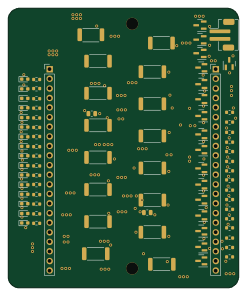
Module 16S PassiveBalanceAddOn
61 × 74 mm86 parts2LCC-BY-NC-4.01.1k
TemperaturePCB PANEL
116 × 75.5 mm178 parts2LCC-BY-NC-4.01.1k
ProgrammingAdapter
10.5 × 83 mm3 parts2LCC-BY-NC-4.01.1k