
Jtag gpio breakout

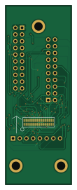
About the Jtag gpio breakout
Jtag gpio breakout is an open source PCB design by erdc, published on GitHub under the SHL-2.1 license. It is a 2-layer board measuring 25 × 67.6 mm, with 4 components from 4 distinct parts.
It belongs with the dev boards & breakouts and usb & debug tools designs in this gallery.
From the project
Deprecated Kicad Board Files for the ACEStat
run git submodule init to get the symbol and footprint libraries
the gerber folder is a placeholder to maintain paths. gerber files are generated via a program and should not be stored in this repo
JTAG GPIO BREAKOUT is a programming connector and an io breakout connector
Citation "ACEstat: A DIY Guide to Unlocking the Potential of Integrated Circuit Potentiostats for Open-Source Electrochemical Analysis" Eric W. Brown, Matthew W. Glasscott, Keith Conley, Jesse Barr, Jason D. Ray, Lee C. Moores, and Anton Netchaev* https://pubs.acs.org/doi/10.1021/acs.analchem.1c04226
Jtag gpio breakout bill of materials (BOM)
4 components, 4 distinct parts — part numbers from the project's BOM.
| Qty | Part | Footprint | Refs |
|---|---|---|---|
| 1 | 70246-2001 Conn_02x04_Odd_Even Molex | PinHeader_2x10_P2.54mm_Vertical | J1 |
| 1 | 203955-0503 Conn_02x25_Odd_Even Molex | Molex_SlimStack_2039550503 | J2 |
| 1 | 22-28-4084 Conn_01x08 Molex | PinHeader_1x08_P2.54mm_Vertical | J3 |
| 1 | 90131-0770 Conn_02x04_Odd_Even Molex | PinHeader_2x10_P2.54mm_Vertical | J4 |
Jtag gpio breakout design files
The KiCad project lives in the erdc/ACEStat_Kicad_Deprecated repository on GitHub; these links point at the commit this page was built from.
Jtag gpio breakout: common questions
How big is the Jtag gpio breakout?
The Jtag gpio breakout measures 25 × 67.6 mm, has 2 copper layers and is 1.6 mm thick.
How many components are on the Jtag gpio breakout?
4 components, from 4 distinct parts, with part numbers taken from the project's own BOM. The full bill of materials is listed on this page.
Where can I download the Jtag gpio breakout design files?
From the erdc/ACEStat_Kicad_Deprecated repository on GitHub, which has the KiCad layout and the BOM; the links under Design files point to each one.
Can I use the Jtag gpio breakout design in my own project?
It is published under SHL-2.1, which limits how it may be reused; read the license before building on it.
More boards in ACEStat_Kicad_Deprecated
Similar boards
Breakout 112pin Connector
rusefi
174 × 58 mm39 parts2LGPL-3.01.2k
134pin 7-967288-1
139.7 × 73.7 mm38 parts2LGPL-3.01.2k
Breakout 60pin EEC-IV
139.7 × 62.2 mm15 parts2LGPL-3.01.2k
Eecv breakout
140.8 × 53.7 mm9 parts4LGPL-3.01.2k
88 Pin Vag Breakout
142 × 58 mm91 parts2LGPL-3.01.2k
Rj45 breakout
rene-dev
15.2 × 53.8 mm3 parts2LGPL-3.0979