
Psu layout v04

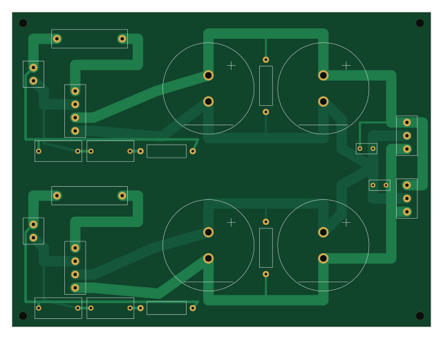
About the Psu layout v04 PCB
Psu layout v04 is an open source PCB design by ewinkuo1-sudo, published on GitHub under the MIT license. It is a 2-layer board measuring 160 × 120 mm, with 26 components from 13 distinct parts.
By type, the board carries 10 capacitors, 4 connectors, 4 resistors and 2 fuses.
It belongs with the audio designs in this gallery, and the repository also holds 1 earlier revision of it.
From the project
LM3886 DIY 純後級:內建線性電源,搭配 Eversolo DAC-Z10 RCA 前級輸出;電路、選材與量測
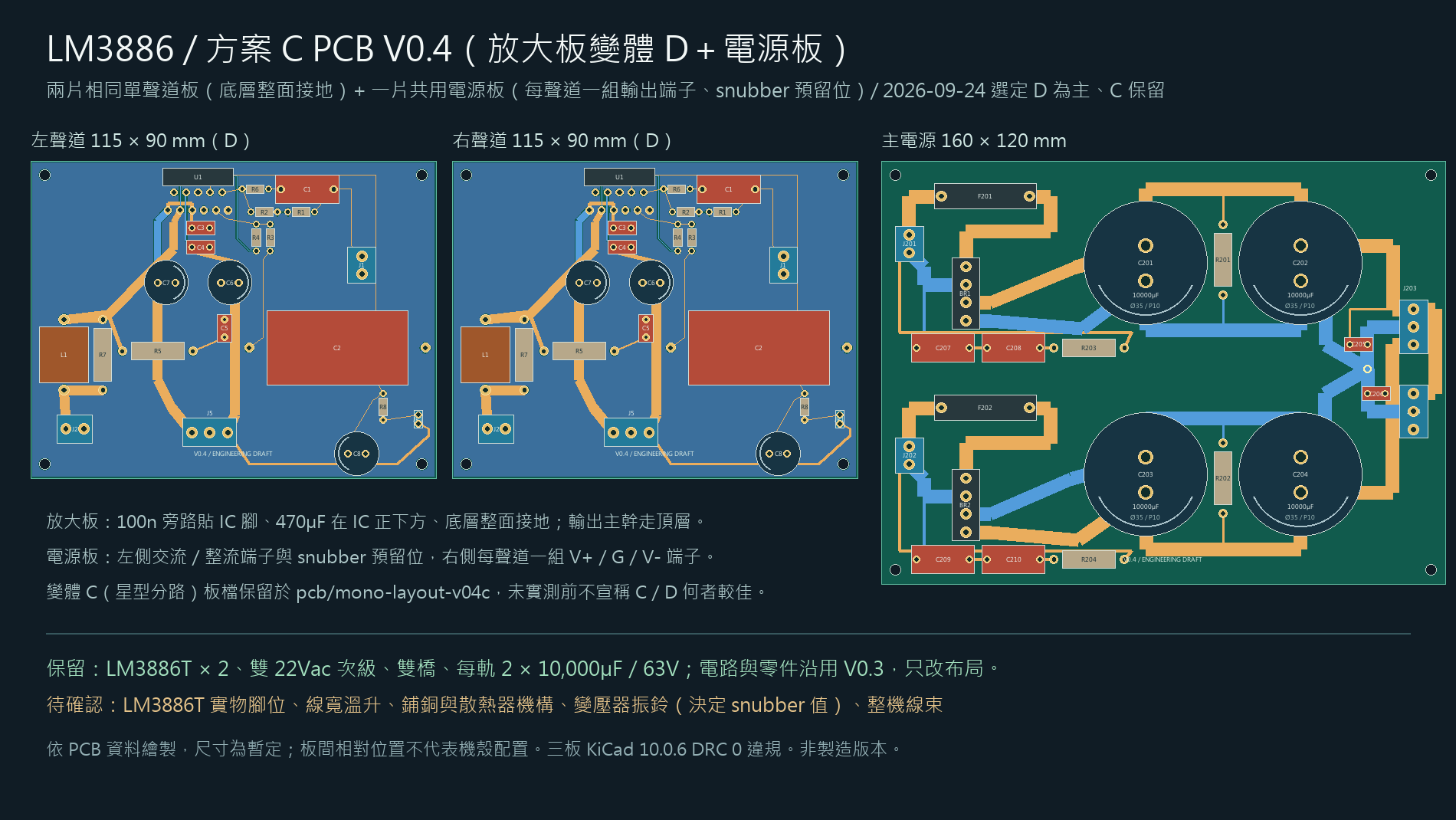
現行版本是 V0.4(2026-09-24:放大板變體 D 為主、變體 C 保留、電源板加每聲道端子與 snubber 預留位),三板 KiCad 10.0.6 DRC 0 違規、0 未連通,見下方「PCB V0.4」各節;正反面銅箔、組裝極性、3D 預覽與零件核對表在 inspection-v04。V0.3 自 2026-09-24 起為歷史版本:板檔、DRC、雜湊綁定與審查結論原樣保留供對照,不再修改。
兩片 100×90 mm 單聲道放大板+一片 160×120 mm 共用電源板。(2026-09-24 放大板已改為 115×90 mm 並重建,DRC 0 違規、0 未連通。)
其他資料:銅箔計算表/完整計算資料與輸入雜湊、驗證摘要、DRC 檔案綁定、正反面/組裝/3D 看圖資料、零件與封裝核對表、左右聲道對照。
Psu layout v04 bill of materials (BOM)
26 components, 13 distinct parts — part numbers from the project's BOM.
| Qty | Part | Footprint | Refs |
|---|---|---|---|
| 1 | T1 SEC 1 | Terminal2_P5.08 | J201 |
| 1 | T1 SEC 2 | Terminal2_P5.08 | J202 |
| 1 | TO L AMP J5 | Terminal3_P5.08 | J203 |
| 1 | TO R AMP J5 | Terminal3_P5.08 | J204 |
| 2 | >=15A / >=200V TBD | BridgeTerminal4_P5.08 | BR1, BR2 |
| 2 | TBD per transformer | Fuse5x20_P25 | F201, F202 |
| 4 | M3 provisional | H1, H2, H3, H4 | |
| 4 | 10000u / 63V | CP_D35_P10 | C201, C202, C203, C204 |
| 2 | 100n / 100V film | Film_P5 | C205, C206 |
| 2 | TBD Cx (10n / 630V film) | Film_P15 | C207, C209 |
| 2 | TBD Cs (150n / 630V film) | Film_P15 | C208, C210 |
| 2 | 2.2k / 2W BLEED | R_2W_P20 | R201, R202 |
| 2 | TBD Rs (10R-47R / 2W) | R_2W_P20 | R203, R204 |
Psu layout v04 design files
The KiCad project lives in the ewinkuo1-sudo/diy-lm3886-amplifier repository on GitHub; these links point at the commit this page was built from.
Psu layout v04: common questions
How big is the Psu layout v04 PCB?
The Psu layout v04 measures 160 × 120 mm, has 2 copper layers and is 1.6 mm thick.
How many components are on the Psu layout v04?
26 components, from 13 distinct parts, with part numbers taken from the project's own BOM. The full bill of materials is listed on this page.
Where can I download the Psu layout v04 design files?
From the ewinkuo1-sudo/diy-lm3886-amplifier repository on GitHub, which has the KiCad layout and the BOM; the links under Design files point to each one.
Can I use the Psu layout v04 design in my own project?
Yes, under the terms of its MIT license, which ewinkuo1-sudo chose for the repository.
More boards in diy-lm3886-amplifier
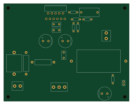
Earlier revisions in the repo: psu-layout-v03
Similar boards
OtterCastAudioV2
Ottercast
50 × 49.3 mm216 parts4LMIT665
FunBox
GuitarML
59.7 × 67.5 mm63 parts2LMIT278
Eurorack pmod
apfaudio
35 × 110 mm116 parts4LCERN-OHL-S-2.0239
XassetteAsterisk
SdtElectronics
56 × 56 mm137 parts2LCERN-OHL-W-2.0229
AddOnC
freeDSP
380 × 45 mm97 parts2LCC-BY-SA-4.0222
AddOnA
178 × 39 mm55 parts2LCC-BY-SA-4.0222