
Universal jlink adapter

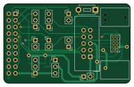
About the Universal jlink adapter PCB
Universal jlink adapter is an open source PCB design by Fescron, published on GitHub under the CERN-OHL-1.2 license. It is a 2-layer board measuring 48.3 × 30.5 mm, with 18 components from 12 distinct parts.
By type, the board carries 10 jumpers, 5 connectors, 1 switch, 1 capacitor and 1 resistor.
It belongs with the usb & debug tools, power & battery and dev boards & breakouts designs in this gallery, and the repository also holds 3 earlier revisions of it.
From the project
20 pin SWD/JTAG J-Link to 10 pin (0.1" and 0.05") reconfigurable Cortex-M header with power supply and TagConnect compatibility, as well as with a reset button. (Info about about J-Link Commander and Segger RTT is also given.)
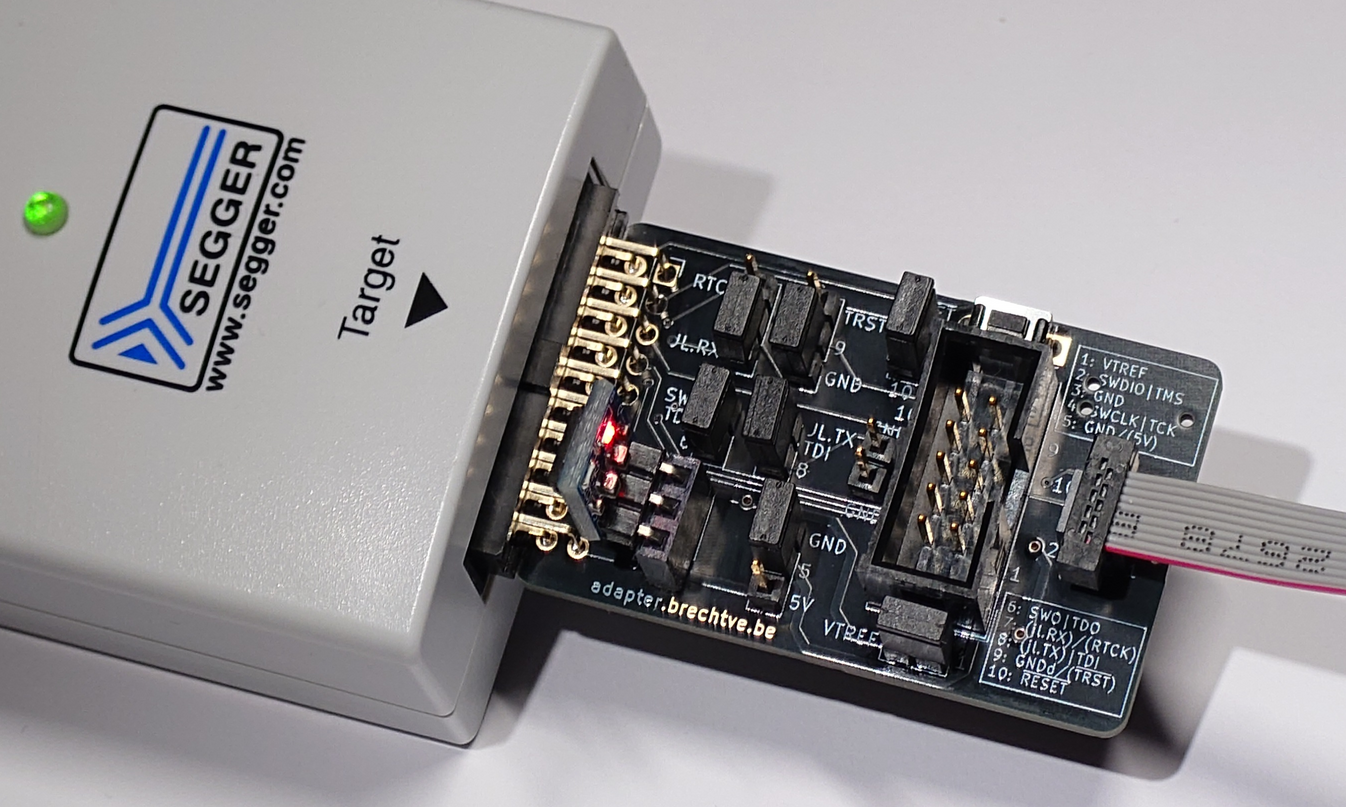
This multifunctional adapter board, primarily designed for use with a J-Link debugger (but others which follow the standard 20-pin JTAG/SWD pinout also work), allows the user to have the standard 9 pin Cortex-M SWD/JTAG pinout on both a 0.1" (2.54mm) and 0.05" (1.27mm) male pinheader. With additional jumpers it is possible to have extra functionality like UART debugging though the J-Link's VCOM on pins which normally aren't used in some modes, if the probe's hardware supports this. Good labeling of all pin numbers and their corresponding functionality also help to speed-up the…
Universal jlink adapter bill of materials (BOM)
18 components, 12 distinct parts.
| Qty | Part | Footprint | Refs |
|---|---|---|---|
| 1 | Conn_02x10_Odd_Even | PinSocket_2x10_P2.54mm_Horizontal | J1 |
| 1 | Conn_02x05_Odd_Even | IDC-Header_2x05_P2.54mm_Vertical | J2 |
| 1 | Conn_02x05_Odd_Even | PinHeader_2x05_P1.27mm_Vertical | J3 |
| 1 | Conn_01x03 | PinSocket_1x03_P2.54mm_Vertical | J4 |
| 1 | Conn_01x02_Pin | PinHeader_1x02_P2.54mm_Vertical | J5 |
| 2 | SolderJumper_3_Bridged12 | SolderJumper-3_P1.3mm_Bridged12_Pad1.0x1.5mm_NumberLabels | JP1, JP2 |
| 3 | Jumper_3_Bridged12 | PinHeader_1x03_P2.54mm_Vertical | JP3, JP6, JP7 |
| 4 | Jumper_2_Bridged | PinHeader_1x02_P2.54mm_Vertical | JP4, JP5, JP8, JP9 |
| 1 | SolderJumper_2_Bridged | SolderJumper-2_P1.3mm_Bridged_Pad1.0x1.5mm | JP10 |
| 1 | SW_Push | SW_PUSH_1P1T_6x3.5mm_H4.3_APEM_MJTP1243 | SW1 |
| 1 | 100 nF | C_0603_1608Metric_Pad1.08x0.95mm_HandSolder | C1 |
| 1 | 100 Ω | R_0603_1608Metric_Pad0.98x0.95mm_HandSolder | R1 |
Universal jlink adapter design files
The KiCad project lives in the Fescron/universal-jlink-adapter repository on GitHub; these links point at the commit this page was built from.
Universal jlink adapter: common questions
How big is the Universal jlink adapter PCB?
The Universal jlink adapter measures 48.3 × 30.5 mm, has 2 copper layers and is 1.6 mm thick.
How many components are on the Universal jlink adapter?
18 components, from 12 distinct parts. The full bill of materials is listed on this page.
Where can I download the Universal jlink adapter design files?
From the Fescron/universal-jlink-adapter repository on GitHub, which has the KiCad layout and the schematic; the links under Design files point to each one.
Can I use the Universal jlink adapter design in my own project?
Yes, under the terms of its CERN-OHL-1.2 license, which Fescron chose for the repository.
Earlier revisions in the repo: jlink-tagConnect-adapter-v3, jlink-tagConnect-adapter-v2, jlink-tagConnect-adapter
Similar boards

Stack chan
stack-chan
50 × 50 mm33 parts2LApache-2.01.7k
Display Carrier
AxxAxx
35.6 × 58.2 mm5 parts2LGPL-3.01.7k
Breakout 60pin EEC-IV
rusefi
139.7 × 62.2 mm15 parts2LGPL-3.01.2k
Eecv breakout
140.8 × 53.7 mm9 parts4LGPL-3.01.2k
134pin 7-967288-1
139.7 × 73.7 mm38 parts2LGPL-3.01.2k
Breakout 112pin Connector
174 × 58 mm39 parts2LGPL-3.01.2k