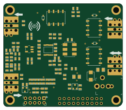
Gm study e1

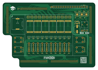
About the Gm study e1 PCB
Gm study e1 is an open source PCB design by fm4dd, published on GitHub under the CERN-OHL-P-2.0 license. It is a 2-layer board measuring 100 × 70 mm, with 105 components from 26 distinct parts.
Other key parts include the SGM6603-5.0 and TXB0104. By type, the board carries 33 resistors, 13 capacitors, 11 LEDs, 10 switches, 4 ICs and 2 jumpers.
It belongs with the dev boards & breakouts and displays & leds designs in this gallery.
From the project
EE education board for the GateMate FPGA evaluation board E1
The gm-study-e1 board is an application module board for the GateMate FPGA evaluation board E1, made by Cologne Chip. It connects to the evaluation board through all six GPIO headers, and its main feature are the input/output components similar to popular FPGA trainer boards used for classroom teaching in electrical engineering and embedded systems education (e.g. Digilent Basys or Altera DE10-lite). These boards were created after successful design tests of the gm-proto-e1 boards. The "gm-proto-e1" boards have only a few basic I/O, but provide a 2.54mm prototyping area for experimentation…
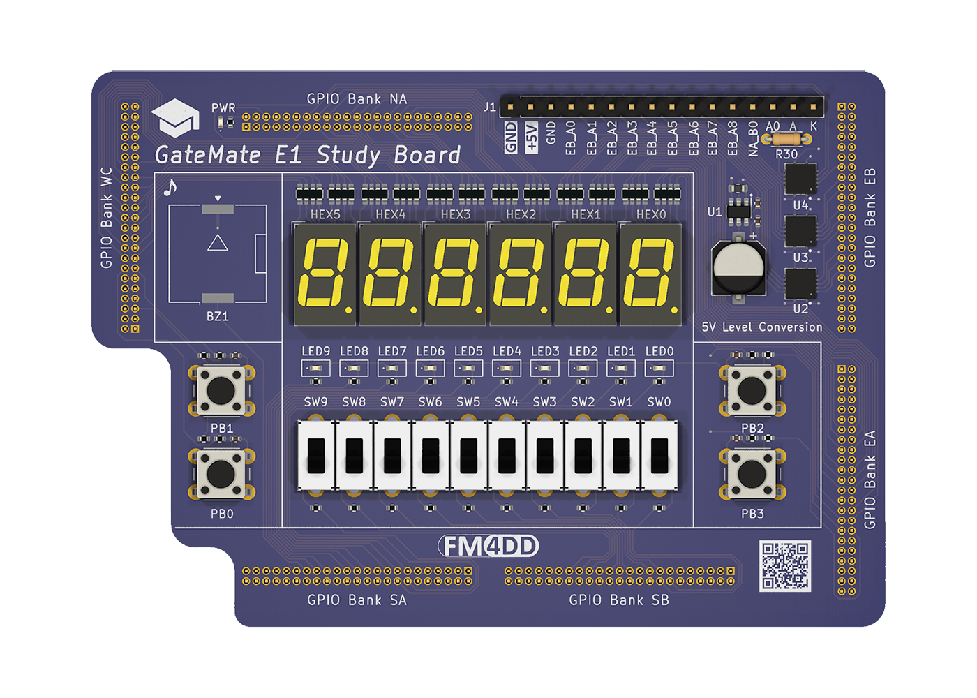
Main components on the Gm study e1
Gm study e1 bill of materials (BOM)
105 components, 26 distinct parts — part numbers from the project's BOM.
| Qty | Part | Footprint | Refs |
|---|---|---|---|
| 1 | SGM6603-5.0 | SOT-23-6 | U1 |
| 3 | TXB0104 TXB104 | S-PVQFN-N14-1EP_3.65x3.65_P0.5_EP2.05x2.05 | U2, U3, U4 |
| 1 | CharLCD_Header | CharLCD Header | J1 |
| 1 | Buzzer | Buzzer_Murata_PKLCS1212E | BZ1 |
| 6 | Hdr_2x23_P1.27 | PinHeader_2x23_P1.27_backside | EA1, EB1, NA1, SA1, SB1, WC1 |
| 6 | 7SEG_SLS0281FR1A1GD | 7SEG SMD SLS0281FR1A1GD | HEX0, HEX1, HEX2, HEX3, HEX4, HEX5 |
| 1 | SolderJumper_2_Open | SolderJumper-2_P1.3mm_Open_Pad1.0x1.5mm | JP1 |
| 1 | UP_PWR | PinHeader_1x03_P2.54mm_Vertical | JP2 |
| 4 | SW_Push | SW_PUSH_6mm | PB0, PB1, PB2, PB3 |
| 12 | 180 | R_Array_Convex_4x0603 | RA1, RA2, RA3, RA4, RA5, RA6, RA7, RA8 +4 |
| 1 | 10K | Potentiometer_Bourns_3362P_Vertical | RV1 |
| 10 | SW_SPDT | SlideSW_SS12-D01 | SW0, SW1, SW2, SW3, SW4, SW5, SW6, SW7 +2 |
| 10 | SMD0402 | LED_0402_FPGA | LED0, LED1, LED2, LED3, LED4, LED5, LED6, LED7 +2 |
| 1 | SMD0402 | LED_0402_no_frame | LED10 |
| 1 | 4.7UH 4.7uH | L_0603_1608Metric | L1 |
| 2 | 10uF | C_0402_1005Metric | C1, C2 |
| 4 | 1u | C_0402_1005Metric | C3, C4, C5, C6 |
| 1 | 100UF 100uF | CP_Elec_6.3x5.3 | C7 |
| 6 | 0.1uF | C_0402_1005Metric | C8, C9, C10, C11, C12, C13 |
| 10 | 100K | R_0402_1005Metric | R1, R2, R3, R4, R5, R6, R7, R8 +2 |
Show 6 more
| Qty | Part | Footprint | Refs |
|---|---|---|---|
| 10 | 200 | R_0402_1005Metric | R11, R12, R13, R14, R15, R16, R17, R18 +2 |
| 4 | 200K | R_0402_1005Metric | R21, R22, R23, R24 |
| 4 | 33 | R_0402_1005Metric | R25, R26, R27, R28 |
| 1 | 160 | R_0402_1005Metric | R29 |
| 1 | 100R 100 | R_0402_1005Metric | R30 |
| 3 | 10K | R_0402_1005Metric | R31, R32, R33 |
Gm study e1 design files
The KiCad project lives in the fm4dd/gm-study-e1 repository on GitHub; these links point at the commit this page was built from.
Gm study e1: common questions
How big is the Gm study e1 PCB?
The Gm study e1 measures 100 × 70 mm, has 2 copper layers and is 1.6 mm thick.
How many components are on the Gm study e1?
105 components, from 26 distinct parts, with part numbers taken from the project's own BOM. The full bill of materials is listed on this page.
Where can I download the Gm study e1 design files?
From the fm4dd/gm-study-e1 repository on GitHub, which has the KiCad layout, the schematic and the BOM; the links under Design files point to each one.
Can I use the Gm study e1 design in my own project?
Yes, under the terms of its CERN-OHL-P-2.0 license, which fm4dd chose for the repository.
 atopile


 AxxAxx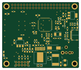
 pa3gsb