
Asic reticulum

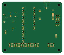
About the Asic reticulum PCB
Asic reticulum is an open source PCB design by gmlewis, published on GitHub under the MIT license. It is a 2-layer board measuring 65 × 56 mm, with 0 components from 0 distinct parts.
It belongs with the rf & radio, power & battery and dev boards & breakouts designs in this gallery.
From the project
SpinalHDL implementation of ASIC hardware for go-reticulum
An Open-Hardware Companion Board for the Reticulum Network Stack with Hardware Cryptographic Acceleration, LoRa Mesh, and Dual-Host Support.
The Universal Reticulum Hat is a high-reliability hardware platform designed to give any Reticulum enthusiast, developer, or emergency responder an instant, pocketable Reticulum communicator.
It bridges the software Reticulum ecosystem (gonomadnet, gorrcd, rnsd) with cutting-edge silicon acceleration (the asic-reticulum Tiny Tapeout ASIC and Gowin Tang Primer 25K FPGA accelerator).
Asic reticulum design files
The KiCad project lives in the gmlewis/asic-reticulum repository on GitHub; these links point at the commit this page was built from.
Asic reticulum: common questions
How big is the Asic reticulum PCB?
The Asic reticulum measures 65 × 56 mm, has 2 copper layers and is 1.6 mm thick.
How many components are on the Asic reticulum?
0 components, from 0 distinct parts, with part numbers taken from the project's own BOM. The full bill of materials is listed on this page.
Where can I download the Asic reticulum design files?
From the gmlewis/asic-reticulum repository on GitHub, which has the KiCad layout, the schematic and the BOM; the links under Design files point to each one.
Can I use the Asic reticulum design in my own project?
Yes, under the terms of its MIT license, which gmlewis chose for the repository.
Similar boards

Display Carrier
AxxAxx
35.6 × 58.2 mm5 parts2LGPL-3.01.7k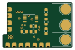
ControllerCurrentShuntAddOn
stuartpittaway
26 × 16.9 mm9 parts2LCC-BY-NC-4.01.1k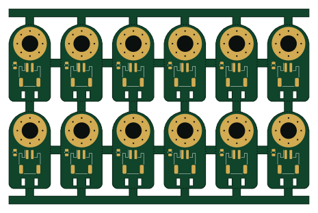
TemperaturePCB PANEL
116 × 75.5 mm178 parts2LCC-BY-NC-4.01.1k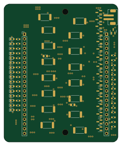
Module 16S PassiveBalanceAddOn
61 × 74 mm86 parts2LCC-BY-NC-4.01.1k
ProgrammingAdapter
10.5 × 83 mm3 parts2LCC-BY-NC-4.01.1k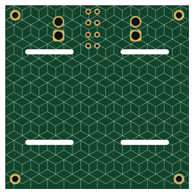
Cube batteryboard
willem-pennings
95 × 95 mm4 parts2LGPL-3.01.1k