
Logic analyzer adapter

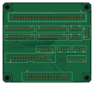
About the Logic analyzer adapter PCB
Logic analyzer adapter is an open source PCB design by hamayanShowa-ele, published on GitHub. It is a 2-layer board measuring 80 × 72 mm, with 14 components from 5 distinct parts.
It belongs with the test & measurement designs in this gallery.
From the project
kicad share data.
Logic analyzer adapter bill of materials (BOM)
14 components, 5 distinct parts.
| Qty | Part | Footprint | Refs |
|---|---|---|---|
| 1 | LAP-C 50pin | cn_HIF3FC-50PA-2.54DSA | CN1 |
| 4 | B10B-XH-A | cn_B10B-XH-A | CN2, CN3, CN4, CN5 |
| 5 | B4B-XH-A | cn_B4B-XH-A | CN6, CN9, CN10, CN13, CN14 |
| 2 | B6B-XH-A | cn_B6B-XH-A | CN7, CN8 |
| 2 | DISCOVERY 30Pin | cn_HIF3FC-30PA-254DSA | CN11, CN12 |
Logic analyzer adapter design files
The KiCad project lives in the hamayanShowa-ele/kicad_share repository on GitHub; these links point at the commit this page was built from.
Logic analyzer adapter: common questions
How big is the Logic analyzer adapter PCB?
The Logic analyzer adapter measures 80 × 72 mm, has 2 copper layers and is 1.6 mm thick.
How many components are on the Logic analyzer adapter?
14 components, from 5 distinct parts. The full bill of materials is listed on this page.
Where can I download the Logic analyzer adapter design files?
From the hamayanShowa-ele/kicad_share repository on GitHub, which has the KiCad layout; the links under Design files point to each one.
Can I use the Logic analyzer adapter design in my own project?
The repository has no license, so all rights stay with hamayanShowa-ele. Use it as a reference, and ask the author before reusing the design.
More boards in kicad_share
 STM32
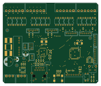
STM322102 DIO 0808
102 × 86 mm227 parts4LNo license0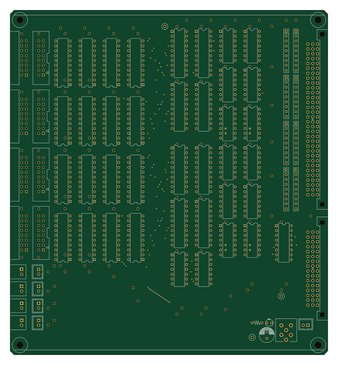
2116 NEW UNIT PULSE IN 64
166 × 180 mm176 parts2LNo license0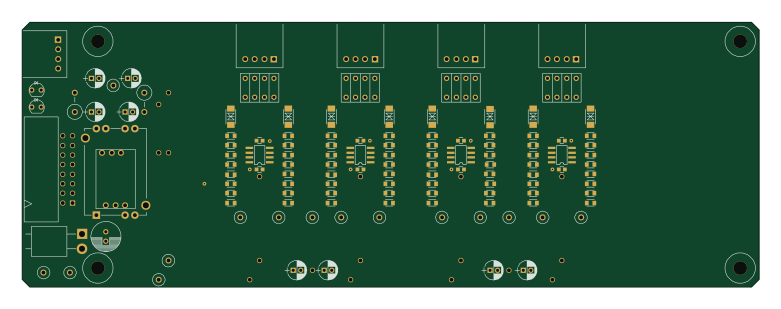
2204 UNIT ANALOG PROTECT BOARD
195 × 70 mm157 parts2LNo license0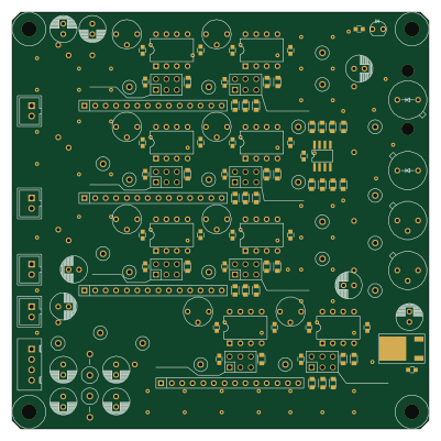
2212 PHOTO DIODE PRE AMP
100 × 100 mm151 parts2LNo license0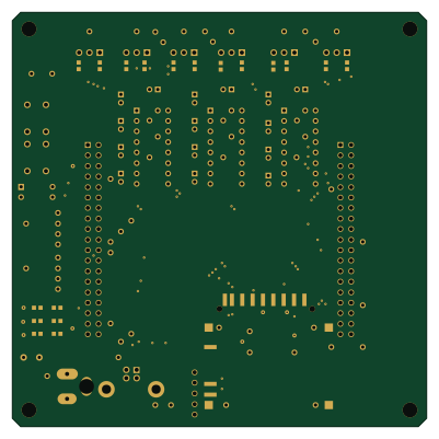
Serial Communication Selector
100 × 100 mm83 parts2LNo license0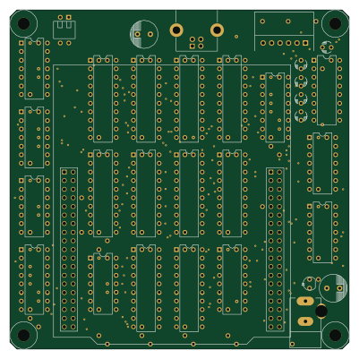
Media converter 02
100 × 100 mm63 parts2LNo license0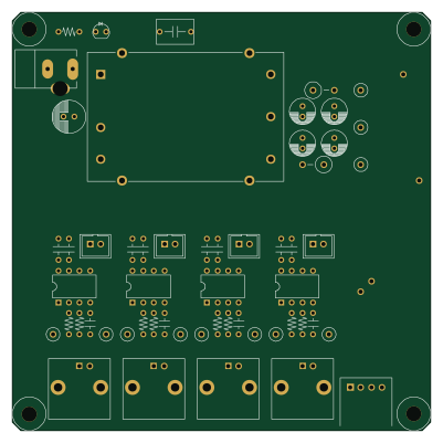
2213 PHOTO DIODE BUFFER AMP
100 × 100 mm56 parts2LNo license0
1812 C-BUS EMULATOR
100 × 148.7 mm56 parts2LNo license0
MatrixLEDcontrol
76 × 92 mm49 parts2LNo license0 ESP32
ESP32ESP DEV BOARD
76 × 92 mm42 parts2LNo license0
AnalogDiscovery2TestBench
80 × 91 mm35 parts2LNo license0
Similar boards
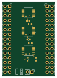
LevelShifter
gusmanb
28.3 × 39.8 mm21 parts2LGPL-3.05.0k
StackLink
52.3 × 10.5 mm5 parts2LGPL-3.05.0k
AnalyzerBoxPCB fork
52.7 × 47.9 mm54 parts4LGPL-3.05.0k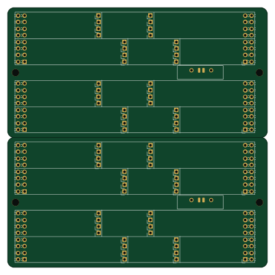
EleLab v2 Bus100
Chrismettal
100 × 100 mm37 parts2LGPL-3.0528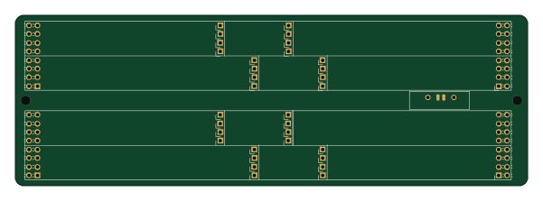
EleLab v2 Bus150
150 × 50 mm37 parts2LGPL-3.0528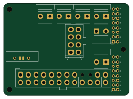
EleLab v2 PowerFeed
68 × 50 mm11 parts2LGPL-3.0528