
PCB-Designs

About the PCB-Designs
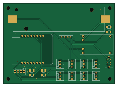
PCB-Designs is an open source ESP8266 PCB design by hmbusch, published on GitHub. It is a 2-layer board measuring 94 × 68 mm, with 19 components from 16 distinct parts.
Its main chip is the WeMos_D1_mini, from the ESP8266 family. By type, the board carries 9 connectors, 3 diodes, 3 resistors, 2 ICs, 1 battery holder and 1 switch.
It belongs with the power & battery and iot & wireless designs in this gallery.
From the project
These are some PCBs I designed and my symbol and footprint libraries (KiCad, EAGLE)
URL: https://github.com/hmbusch/PCB-Designs
From time to time I sit down and design some circuitry that can be used for multiple purposes, a component if you will. The designs for these PCBs are stored in this project (or at least those I feel confident to share).
I started out developing a basic two button remote that I could use together with Home Assistant. I expected the design to go through various iterations as I try different functionality, so instead of designing several completely different iterations, I created a sort of universal motherboard. It breaks out almost all pins as…
Main components on the PCB-Designs
PCB-Designs bill of materials (BOM)
19 components, 16 distinct parts.
| Qty | Part | Footprint | Refs |
|---|---|---|---|
| 1 | WeMos_D1_mini | WEMOS_D1_mini_light | U1 |
| 1 | ~ | TP4056-Module | U2 |
| 1 | Conn_I2C | Molex_KK-254_AE-6410-04A_1x04_P2.54mm_Vertical | J1 |
| 1 | Conn_D0 | Molex_KK-254_AE-6410-03A_1x03_P2.54mm_Vertical | J2 |
| 1 | Conn_D7 | Molex_KK-254_AE-6410-03A_1x03_P2.54mm_Vertical | J3 |
| 1 | Conn_D8 | Molex_KK-254_AE-6410-03A_1x03_P2.54mm_Vertical | J4 |
| 1 | Conn_A0 | Molex_KK-254_AE-6410-03A_1x03_P2.54mm_Vertical | J5 |
| 1 | Conn_D4 | Molex_KK-254_AE-6410-03A_1x03_P2.54mm_Vertical | J6 |
| 1 | Conn_D3 | Molex_KK-254_AE-6410-03A_1x03_P2.54mm_Vertical | J7 |
| 1 | Conn_D5 | Molex_KK-254_AE-6410-03A_1x03_P2.54mm_Vertical | J8 |
| 1 | Conn_D6 | Molex_KK-254_AE-6410-03A_1x03_P2.54mm_Vertical | J9 |
| 1 | 18650 LiPo | BatteryHolder_Keystone_1042_1x18650_different_silkscreen | BT1 |
| 1 | SW_LOAD | SK22D07_DPDT_slide_switch | SW4 |
| 2 | LED | LED_SMD_3528_1411 | D1, D2 |
| 1 | Power LED | LED_SMD_3528_1411 | D3 |
| 3 | 120 | R_1206_3216Metric_Pad1.30x1.75mm_HandSolder | R1, R2, R3 |
PCB-Designs design files
The KiCad project lives in the hmbusch/PCB-Designs repository on GitHub; these links point at the commit this page was built from.
PCB-Designs: common questions
What microcontroller does the PCB-Designs use?
The PCB-Designs is built around the WeMos_D1_mini, from the ESP8266 family.
How big is the PCB-Designs?
The PCB-Designs measures 94 × 68 mm, has 2 copper layers and is 1.6 mm thick.
How many components are on the PCB-Designs?
19 components, from 16 distinct parts. The full bill of materials is listed on this page.
Where can I download the PCB-Designs design files?
From the hmbusch/PCB-Designs repository on GitHub, which has the KiCad layout and the schematic; the links under Design files point to each one.
Can I use the PCB-Designs design in my own project?
The repository has no license, so all rights stay with hmbusch. Use it as a reference, and ask the author before reusing the design.
Can I test firmware for the PCB-Designs without the hardware?
Yes. HardLabs builds a simulation of the board from its netlist and BOM, so you can run and debug ESP8266 firmware against it before you order a PCB.
Similar boards
 ESP8266
ESP8266ControllerCircuit
stuartpittaway
75 × 30 mm20 parts2LCC-BY-NC-4.01.1k ESP8266
HASwitchPlate
aderusha
60 × 40 mm8 parts2LMIT738 ESP8266
RatGDO-OpenSource-D1Mini-ESP8266
Kaldek
47.8 × 63.3 mm12 parts2LMIT506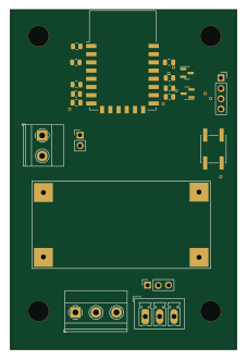 ESP8266
RatGDO-OpenSource-Bare-ESP8266
55 × 82.7 mm20 parts2LMIT506 ESP8266
Goatgdo
32.9 × 53.3 mm23 parts2LMIT506 ESP8266
Iaq board
nkitanov
70.1 × 43.2 mm17 parts2LNo license398