
Casio VX Debug Unit

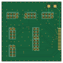
About the Casio VX Debug Unit PCB
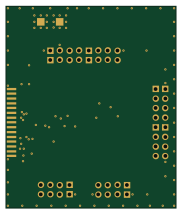
Casio VX Debug Unit is an open source PCB design by hwreverse, published on GitHub under the MIT license. It is a 2-layer board measuring 51.6 × 51.8 mm, with 17 components from 10 distinct parts.
It belongs with the dev boards & breakouts and retro computing designs in this gallery.
From the project
Breakout & Debug Boards for Vintage Pocket Computers (ポケコン) from Casio, Sharp,... and their Accessories
SALEAE Logic Analyzer friendly (Ground pins with every Bus Pin, Groups of 2x4)
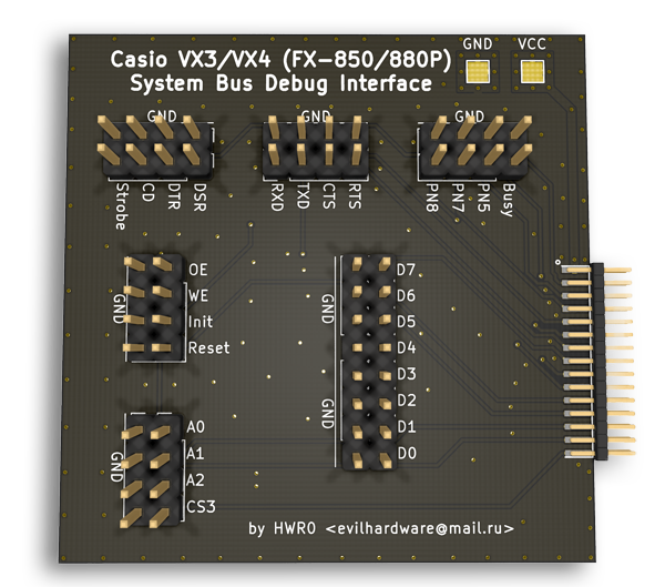
Casio VX Debug Unit bill of materials (BOM)
17 components, 10 distinct parts.
| Qty | Part | Footprint | Refs |
|---|---|---|---|
| 7 | GND | PinHeader_1x04_P2.54mm_Vertical | J1, J5, J7, J8, J11, J12, J13 |
| 2 | SolidPad-Connector | SolidPad_4x4mm_2x2mmCore | J2, J3 |
| 1 | Busy+PN | PinHeader_1x04_P2.54mm_Vertical | J4 |
| 1 | CASIO_VX_2x15_1.27_Interface | Connector_Casio_2x15_1.27_SYSBUS | J6 |
| 1 | ADDR+CS | PinHeader_1x04_P2.54mm_Vertical | J9 |
| 1 | Enables+Init+Reset | PinHeader_1x04_P2.54mm_Vertical | J10 |
| 1 | D0-D3 | PinHeader_1x04_P2.54mm_Vertical | J14 |
| 1 | D4-D7 | PinHeader_1x04_P2.54mm_Vertical | J15 |
| 1 | Serial 1 | PinHeader_1x04_P2.54mm_Vertical | J16 |
| 1 | Serial 2 + Strobe | PinHeader_1x04_P2.54mm_Vertical | J17 |
Casio VX Debug Unit design files
The KiCad project lives in the hwreverse/PokeconDebug repository on GitHub; these links point at the commit this page was built from.
Casio VX Debug Unit: common questions
How big is the Casio VX Debug Unit PCB?
The Casio VX Debug Unit measures 51.6 × 51.8 mm, has 2 copper layers and is 0.8 mm thick.
How many components are on the Casio VX Debug Unit?
17 components, from 10 distinct parts. The full bill of materials is listed on this page.
Where can I download the Casio VX Debug Unit design files?
From the hwreverse/PokeconDebug repository on GitHub, which has the KiCad layout; the links under Design files point to each one.
Can I use the Casio VX Debug Unit design in my own project?
Yes, under the terms of its MIT license, which hwreverse chose for the repository.
More boards in PokeconDebug
Similar boards
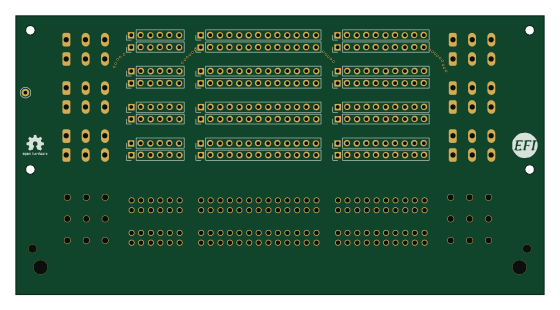
134pin 7-967288-1
rusefi
139.7 × 73.7 mm38 parts2LGPL-3.01.2k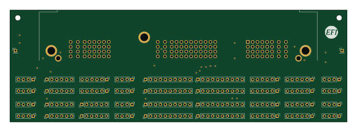
Breakout 112pin Connector
174 × 58 mm39 parts2LGPL-3.01.2k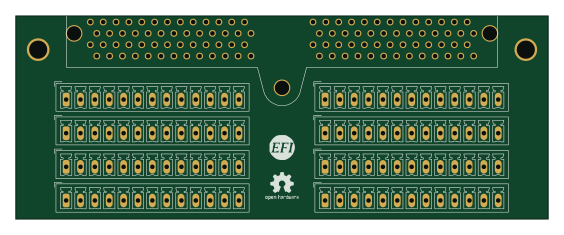
Eecv breakout
140.8 × 53.7 mm9 parts4LGPL-3.01.2k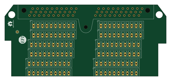
Breakout 60pin EEC-IV
139.7 × 62.2 mm15 parts2LGPL-3.01.2k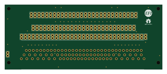
88 Pin Vag Breakout
142 × 58 mm91 parts2LGPL-3.01.2k
Expansion Card Retrofit
FrameworkComputer
24 × 27.3 mm5 parts2LCC-BY-4.01.1k