
MyPad

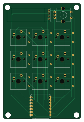
About the MyPad PCB
MyPad is an open source RP2040/RP2350 PCB design by isaaclau888, published on GitHub. It is a 2-layer board measuring 67 × 99.5 mm, with 21 components from 5 distinct parts.
Its main chip is the XIAO-RP2040-DIP, from the RP2040/RP2350 family. By type, the board carries 10 switches, 9 diodes, 1 IC and 1 connector.
It belongs with the keyboards designs in this gallery.
From the project
MyPad is a tiny, pocket-sized macro pad I designed to clear up my desk and speed up my workflow. It has 9 mechanical keys, a vertical screen, and a dial knob, all packed into a super clean layout inspired by the classic look of the original 2001 Apple iPod. Instead of having a ma
MyPad is a tiny, pocket-sized macro pad I designed to clear up my desk and speed up my workflow. It has 9 mechanical keys, a vertical screen, and a dial knob, all packed into a super clean layout inspired by the classic look of the original 2001 Apple iPod. Instead of having a massive grid of keys, MyPad relies on clever software. By using multiple code layers and custom shortcuts, this little 3x3 pad can handle everything from jumping through complex lines of code in VS Code to tweaking 3D models in Fusion 360, all without my hand ever leaving the controller.
Main components on the MyPad
MyPad bill of materials (BOM)
21 components, 5 distinct parts — part numbers from the project's BOM.
| Qty | Part | Footprint | Refs |
|---|---|---|---|
| 1 | XIAO-RP2040-DIP | XIAO-RP2040-DIP | U1 |
| 1 | Conn_01x04_Pin | SSD1306-0.91-OLED-4pin-128x32 | J1 |
| 9 | SW_Push | SW_Cherry_MX_1.00u_PCB | SW1, SW2, SW3, SW4, SW5, SW6, SW7, SW8 +1 |
| 1 | RotaryEncoder_Switch | RotaryEncoder_Alps_EC11E-Switch_Vertical_H20mm | SW10 |
| 9 | 1N4148 | D_DO-35_SOD27_P7.62mm_Horizontal | D1, D2, D3, D4, D5, D6, D7, D8 +1 |
MyPad design files
The KiCad project lives in the isaaclau888/MyPad repository on GitHub; these links point at the commit this page was built from.
MyPad: common questions
What microcontroller does the MyPad use?
The MyPad is built around the XIAO-RP2040-DIP, from the RP2040/RP2350 family.
How big is the MyPad PCB?
The MyPad measures 67 × 99.5 mm, has 2 copper layers and is 1.6 mm thick.
How many components are on the MyPad?
21 components, from 5 distinct parts, with part numbers taken from the project's own BOM. The full bill of materials is listed on this page.
Where can I download the MyPad design files?
From the isaaclau888/MyPad repository on GitHub, which has the KiCad layout, the schematic and the BOM; the links under Design files point to each one.
Can I use the MyPad design in my own project?
The repository has no license, so all rights stay with isaaclau888. Use it as a reference, and ask the author before reusing the design.
Can I test firmware for the MyPad without the hardware?
Yes. HardLabs builds a simulation of the board from its netlist and BOM, so you can run and debug RP2040/RP2350 firmware against it before you order a PCB.
Similar boards
 RP2040/RP2350
Open Book Abridged Edition
joeycastillo
85 × 115 mm29 parts2LCC-BY-SA-4.08.1k RP2040/RP2350
Corne
foostan
277.2 × 107.5 mm164 parts2LCC-BY-4.07.7k RP2040/RP2350
Corne
277.2 × 107.5 mm164 parts2LCC-BY-4.07.7k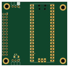 RP2040/RP2350
LogicAnalyzer
gusmanb
57 × 55.2 mm6 parts2LGPL-3.05.0k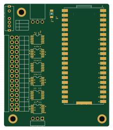 RP2040/RP2350
Jitx design
55.5 × 65 mm26 parts4LGPL-3.05.0k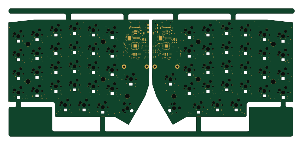 RP2040/RP2350
Pro V2
kata0510
290.1 × 130 mm270 parts2LMIT2.3k