
Fascia

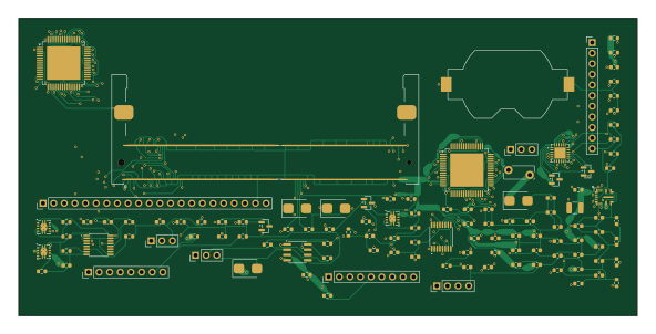
About the Fascia PCB
Fascia is an open source PCB design by jessiepullaro414, published on GitHub under the MIT license. It is a 6-layer board measuring 147.8 × 71.1 mm, with 118 components from 87 distinct parts.
Other key parts include the LM74930-Q1, LM61460-Q1, TLV767-Q1, TCAN1044V-Q1 and SN65DSI85-Q1. By type, the board carries 49 resistors, 39 capacitors, 10 ICs, 10 connectors, 4 transistors and 4 diodes.
It belongs with the audio and iot & wireless designs in this gallery.
From the project
Companion KiCad project for "Fascia", a 10-inch Android Automotive touch display head unit: sibling to manifold-pcb, thermo-pcb and ecu-pcb, same 12V automotive constraints as the rest of the family.
Companion KiCad project for "Fascia", a 10-inch Android Automotive touch display head unit: sibling to manifold-pcb, thermo-pcb and ecu-pcb, same 12V automotive constraints as the rest of the family.
Unlike the rest of the family this is a two-board project, because the panel is physically detached from the main board and sits across the dash from it:
1. Carrier board (behind the dash) — a Toradex Verdin iMX95 System on Module on a custom carrier: automotive 12V front end, LVDS display output via a DSI-to-LVDS bridge, backlight control, CAN FD to talk to ecu-pcb, line-level audio pre-outs…
Main components on the Fascia
Fascia bill of materials (BOM)
118 components, 87 distinct parts.
| Qty | Part | Footprint | Refs |
|---|---|---|---|
| 1 | LM74930-Q1 | Texas_RGE0024H_VQFN-24-1EP_4x4mm_P0.5mm_EP2.7x2.7mm | U1 |
| 1 | LM61460-Q1 | TI_RJR0014A_VQFN-HR-14_4x3.5mm | U2 |
| 1 | TLV767-Q1 | Texas_DRB0008A | U3 |
| 1 | TCAN1044V-Q1 | SOIC-8_3.9x4.9mm_P1.27mm | U4 |
| 1 | SN65DSI85-Q1 | Texas_TQFP-64-1EP_10x10mm_P0.5mm_EP8x8mm_Mask4.44x4.44mm | U5 |
| 1 | TLV767-Q1 3V3 | Texas_DRB0008A | U6 |
| 2 | SN74AXC4T245-Q1 | TSSOP-16_4.4x5mm_P0.65mm | U7, U8 |
| 1 | PCM3168A-Q1 | Texas_TQFP-64-1EP_10x10mm_P0.5mm_EP8x8mm_Mask4.44x4.44mm | U9 |
| 1 | TPS2557-Q1 | Texas_DRB0008A | U10 |
| 1 | NFET diode | SOT-23 | Q1 |
| 1 | NFET pass | SOT-23 | Q2 |
| 2 | NFET i2c xlat | SOT-23 | Q3, Q4 |
| 1 | Verdin iMX95 | SODIMM-260_DDR4_H4.0-5.2_OrientationStd_Socket | J1 |
| 1 | Power in | PinHeader_1x03_P2.54mm_Vertical | J2 |
| 1 | CAN to ECU | PinHeader_1x03_P2.54mm_Vertical | J3 |
| 1 | Panel LVDS (provisional) | PinHeader_1x22_P2.54mm_Vertical | J4 |
| 1 | Pre-outs to amp | PinHeader_1x11_P2.54mm_Vertical | J5 |
| 1 | Mic | PinHeader_1x03_P2.54mm_Vertical | J6 |
| 1 | USB-C CarPlay | PinHeader_1x09_P2.54mm_Vertical | J7 |
| 1 | JTAG debug | PinHeader_1x08_P2.54mm_Vertical | J8 |
Show 67 more
| Qty | Part | Footprint | Refs |
|---|---|---|---|
| 1 | Buttons | PinHeader_1x04_P2.54mm_Vertical | J9 |
| 1 | RTC coin cell | BatteryHolder_Keystone_1058_1x2032 | J10 |
| 1 | 5A | Fuse_Bourns_MF-RG300 | F1 |
| 1 | TVS 33V | D_SMB | D1 |
| 1 | ESD DP | D_SMB | D2 |
| 1 | ESD DN | D_SMB | D3 |
| 1 | ESD VBUS | D_SMB | D4 |
| 1 | 2.2u | L_1210_3225Metric | L1 |
| 1 | 100uF | C_0603_1608Metric | C1 |
| 1 | 100n CVS | C_0603_1608Metric | C2 |
| 1 | 100n CCAP | C_0603_1608Metric | C3 |
| 1 | open CT | C_0603_1608Metric | C4 |
| 3 | 10u in | C_0603_1608Metric | C5, C9, C22 |
| 1 | 1u VCC | C_0603_1608Metric | C6 |
| 1 | 100n boot | C_0603_1608Metric | C7 |
| 1 | 44u out | C_0603_1608Metric | C8 |
| 2 | 10u out | C_0603_1608Metric | C10, C23 |
| 1 | 100n VCC | C_0603_1608Metric | C11 |
| 1 | 100n VIO | C_0603_1608Metric | C12 |
| 1 | 4n7 split | C_0603_1608Metric | C13 |
| 1 | 1u VCORE | C_0603_1608Metric | C14 |
| 1 | 10u 1V8 | C_0603_1608Metric | C15 |
| 6 | 100n 1V8 | C_0603_1608Metric | C16, C17, C18, C19, C20, C21 |
| 1 | 100n U7A | C_0603_1608Metric | C24 |
| 1 | 100n U7B | C_0603_1608Metric | C25 |
| 1 | 100n U8A | C_0603_1608Metric | C26 |
| 1 | 100n U8B | C_0603_1608Metric | C27 |
| 3 | 10u decouple | C_0603_1608Metric | C28, C29, C30 |
| 4 | 100n codec | C_0603_1608Metric | C31, C32, C33, C34 |
| 1 | 100n RST | C_0603_1608Metric | C35 |
| 1 | 1u couple | C_0603_1608Metric | C36 |
| 1 | 100n IN | C_0603_1608Metric | C37 |
| 1 | 150u VBUS | C_0603_1608Metric | C38 |
| 1 | 100n | C_0603_1608Metric | C39 |
| 1 | 2m sense | R_0603_1608Metric | R1 |
| 1 | 50R | R_0603_1608Metric | R2 |
| 1 | RILIM | R_0603_1608Metric | R3 |
| 1 | 5k RMON | R_0603_1608Metric | R4 |
| 1 | OV top | R_0603_1608Metric | R5 |
| 1 | OV bot | R_0603_1608Metric | R6 |
| 1 | UV top | R_0603_1608Metric | R7 |
| 1 | UV bot | R_0603_1608Metric | R8 |
| 1 | RBOOT | R_0603_1608Metric | R9 |
| 3 | FB top | R_0603_1608Metric | R10, R17, R23 |
| 3 | FB bot | R_0603_1608Metric | R11, R18, R24 |
| 1 | RT | R_0603_1608Metric | R12 |
| 1 | EN top | R_0603_1608Metric | R13 |
| 1 | EN bot | R_0603_1608Metric | R14 |
| 2 | 100k FLT pu | R_0603_1608Metric | R15, R38 |
| 1 | 100k PG pu | R_0603_1608Metric | R16 |
| 2 | 60R term | R_0603_1608Metric | R19, R20 |
| 1 | 10k STB pd | R_0603_1608Metric | R21 |
| 1 | 10k REFCLK | R_0603_1608Metric | R22 |
| 4 | 2k2 pullup | R_0603_1608Metric | R25, R26, R27, R28 |
| 1 | 100k RST | R_0603_1608Metric | R29 |
| 1 | 2k2 mic bias | R_0603_1608Metric | R30 |
| 2 | 10k bias | R_0603_1608Metric | R31, R32 |
| 4 | 10k tie-off | R_0603_1608Metric | R33, R34, R35, R36 |
| 1 | 36k ILIM | R_0603_1608Metric | R37 |
| 1 | 10k Rp CC1 | R_0603_1608Metric | R39 |
| 1 | 10k Rp CC2 | R_0603_1608Metric | R40 |
| 1 | 0R ID | R_0603_1608Metric | R41 |
| 1 | 100k Vsense | R_0603_1608Metric | R42 |
| 1 | 56k Vsense | R_0603_1608Metric | R43 |
| 4 | 10k pullup | R_0603_1608Metric | R44, R45, R46, R47 |
| 1 | 10k JTAG Vref | R_0603_1608Metric | R48 |
| 1 | 47k min | R_0603_1608Metric | R49 |
Fascia design files
The KiCad project lives in the jessiepullaro414/Fascia repository on GitHub; these links point at the commit this page was built from.
- LayoutFascia.kicad_pcb
- SchematicFascia.kicad_sch
Fascia: common questions
How big is the Fascia PCB?
The Fascia measures 147.8 × 71.1 mm, has 6 copper layers and is 1.6 mm thick.
How many components are on the Fascia?
118 components, from 87 distinct parts. The full bill of materials is listed on this page.
Where can I download the Fascia design files?
From the jessiepullaro414/Fascia repository on GitHub, which has the KiCad layout and the schematic; the links under Design files point to each one.
Can I use the Fascia design in my own project?
Yes, under the terms of its MIT license, which jessiepullaro414 chose for the repository.
Similar boards
EinkPDA screen
TalismanDesign
95 × 54 mm27 parts2LApache-2.02.0k
KLOR
GEIGEIGEIST
160.2 × 118.3 mm79 parts2LGPL-3.01.2k
RPi RM0 WiFi/Bluetooth Module
schlae
11.1 × 14 mm76 parts6LNo license1.0k
ButtonsLEDs
shanteacontrols
390 × 37 mm82 parts2LApache-2.0956
Pots
390 × 93 mm75 parts2LApache-2.0956
USB
52 × 12.6 mm6 parts2LApache-2.0956