
M5StampS3 Breakout 4Layer

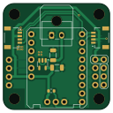
About the M5StampS3 Breakout 4Layer
M5StampS3 Breakout 4Layer is an open source PCB design by JoelEB, published on GitHub. It is a 4-layer board measuring 31.9 × 31.8 mm, with 18 components from 9 distinct parts.
Other key parts include the XC6220B331MR. By type, the board carries 7 connectors, 3 resistors, 2 ICs and 2 capacitors.
It belongs with the iot & wireless and dev boards & breakouts designs in this gallery.
Main components on the M5StampS3 Breakout 4Layer
M5StampS3 Breakout 4Layer bill of materials (BOM)
18 components, 9 distinct parts.
| Qty | Part | Footprint | Refs |
|---|---|---|---|
| 1 | ~ | STAMP-S3-2_54-SOCKET | U1 |
| 1 | XC6220B331MR | SOT-23-5 | U4 |
| 1 | Conn_01x02 | Molex_Micro-Fit_3.0_43650-0200_1x02_P3.00mm_Horizontal | J1 |
| 2 | Qwiic_RA | JST04_1MM_RA | J2, J3 |
| 1 | Conn_01x03 | 1X03 | J4 |
| 3 | Conn_01x04 | 1X04 | J5, J6, J7 |
| 4 | Stand_off | STAND-OFF | ST1, ST2, ST3, ST4 |
| 2 | 10UF | C_1206_3216Metric | C1, C2 |
| 3 | 4.7k | R_0603_1608Metric | R1, R2, R3 |
M5StampS3 Breakout 4Layer design files
The KiCad project lives in the JoelEB/ESP_Smart_Home repository on GitHub; these links point at the commit this page was built from.
M5StampS3 Breakout 4Layer: common questions
How big is the M5StampS3 Breakout 4Layer?
The M5StampS3 Breakout 4Layer measures 31.9 × 31.8 mm, has 4 copper layers and is 1.6 mm thick.
How many components are on the M5StampS3 Breakout 4Layer?
18 components, from 9 distinct parts. The full bill of materials is listed on this page.
Where can I download the M5StampS3 Breakout 4Layer design files?
From the JoelEB/ESP_Smart_Home repository on GitHub, which has the KiCad layout; the links under Design files point to each one.
Can I use the M5StampS3 Breakout 4Layer design in my own project?
The repository has no license, so all rights stay with JoelEB. Use it as a reference, and ask the author before reusing the design.
More boards in ESP_Smart_Home
Similar boards
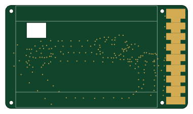
EinkPDA screen
TalismanDesign
95 × 54 mm27 parts2LApache-2.02.0k
Breakout 112pin Connector
rusefi
174 × 58 mm39 parts2LGPL-3.01.2k
Breakout 60pin EEC-IV
139.7 × 62.2 mm15 parts2LGPL-3.01.2k
Eecv breakout
140.8 × 53.7 mm9 parts4LGPL-3.01.2k
88 Pin Vag Breakout
142 × 58 mm91 parts2LGPL-3.01.2k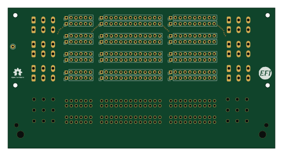
134pin 7-967288-1
139.7 × 73.7 mm38 parts2LGPL-3.01.2k