
AP63200WU Buck convertor

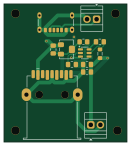
About the AP63200WU Buck convertor PCB
AP63200WU Buck convertor is an open source PCB design by Kartik9250, published on GitHub under the MIT license. It is a 2-layer board measuring 32.5 × 36.5 mm, with 13 components from 11 distinct parts.
Other key parts include the AP63200WU. By type, the board carries 5 capacitors, 4 connectors, 1 IC, 1 inductor and 1 resistor.
It belongs with the power & battery designs in this gallery.
From the project
A variable output synchronous buck converter designed as a practice PCB based on AP63200 in KiCad. Takes a USB-C input and delivers a tunable regulated output over USB-A and screw terminals.
A variable output synchronous buck converter designed as a practice PCB in KiCad. Takes a USB-C input and delivers a tunable regulated output over USB-A and screw terminals.
The AP63200WU is a synchronous buck regulator. It switches an internal MOSFET at high frequency, and the inductor + output capacitors smooth that into a steady DC output.
Output voltage is set by a resistor divider on the feedback (FB) pin:
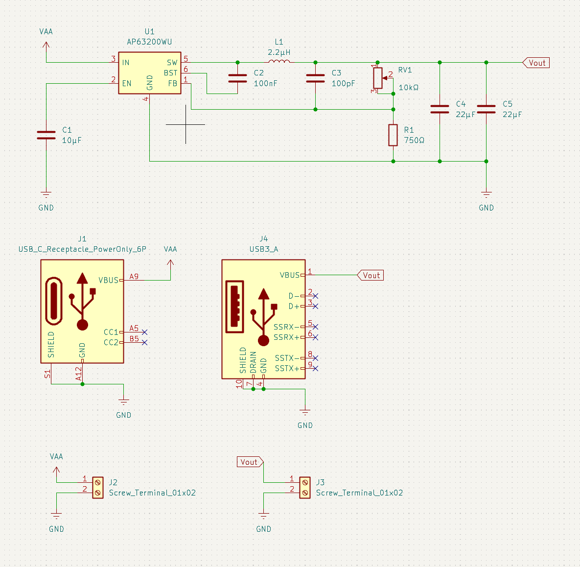
Main components on the AP63200WU Buck convertor
AP63200WU Buck convertor bill of materials (BOM)
13 components, 11 distinct parts.
| Qty | Part | Footprint | Refs |
|---|---|---|---|
| 1 | AP63200WU | TSOT-23-6 | U1 |
| 1 | USB_C_Receptacle_PowerOnly_6P | USB_C_Receptacle_GCT_USB4125-xx-x_6P_TopMnt_Horizontal | J1 |
| 2 | Screw_Terminal_01x02 | TerminalBlock_Xinya_XY308-2.54-2P_1x02_P2.54mm_Horizontal | J2, J3 |
| 1 | USB3_A | USB3_A_Receptacle_Wuerth_692122030100 | J4 |
| 1 | 10kΩ | Potentiometer_Bourns_3224W_Vertical | RV1 |
| 1 | 2.2μH | L_0805_2012Metric_Pad1.05x1.20mm_HandSolder | L1 |
| 1 | 10μF | C_0805_2012Metric_Pad1.18x1.45mm_HandSolder | C1 |
| 1 | 100nF | C_0805_2012Metric_Pad1.18x1.45mm_HandSolder | C2 |
| 1 | 100pF | C_0805_2012Metric_Pad1.18x1.45mm_HandSolder | C3 |
| 2 | 22μF | C_0805_2012Metric_Pad1.18x1.45mm_HandSolder | C4, C5 |
| 1 | 750Ω | R_0805_2012Metric_Pad1.20x1.40mm_HandSolder | R1 |
AP63200WU Buck convertor design files
The KiCad project lives in the Kartik9250/AP63200WU_Buck_convertor repository on GitHub; these links point at the commit this page was built from.
- Layoutbuck_convertor.kicad_pcb
- Schematicbuck_convertor.kicad_sch
AP63200WU Buck convertor: common questions
How big is the AP63200WU Buck convertor PCB?
The AP63200WU Buck convertor measures 32.5 × 36.5 mm, has 2 copper layers and is 1.6 mm thick.
How many components are on the AP63200WU Buck convertor?
13 components, from 11 distinct parts. The full bill of materials is listed on this page.
Where can I download the AP63200WU Buck convertor design files?
From the Kartik9250/AP63200WU_Buck_convertor repository on GitHub, which has the KiCad layout and the schematic; the links under Design files point to each one.
Can I use the AP63200WU Buck convertor design in my own project?
Yes, under the terms of its MIT license, which Kartik9250 chose for the repository.
Similar boards
EinkPDA screen
TalismanDesign
95 × 54 mm27 parts2LApache-2.02.0k
Stack chan
stack-chan
50 × 50 mm33 parts2LApache-2.01.7k
Display Carrier
AxxAxx
35.6 × 58.2 mm5 parts2LGPL-3.01.7k
Module 16S PassiveBalanceAddOn
stuartpittaway
61 × 74 mm86 parts2LCC-BY-NC-4.01.1k
TemperaturePCB PANEL
116 × 75.5 mm178 parts2LCC-BY-NC-4.01.1k
ProgrammingAdapter
10.5 × 83 mm3 parts2LCC-BY-NC-4.01.1k