
Kicad

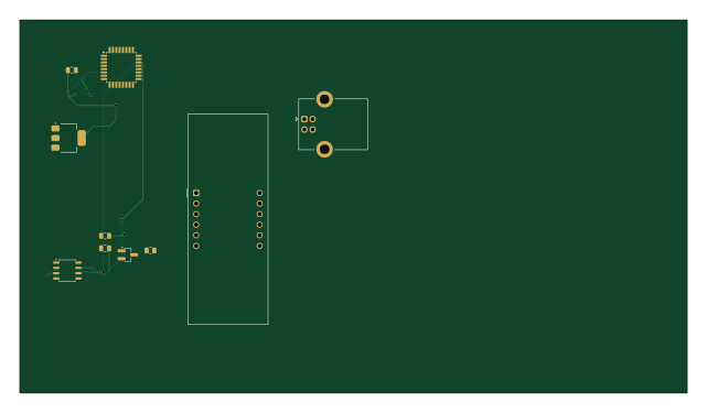
About the Kicad PCB
Kicad is an open source STM32 PCB design by Larryhul, published on GitHub under the MIT license. It is a 2-layer board measuring 160 × 89.5 mm, with 10 components from 8 distinct parts.
Its main chip is the STM32G030K6Tx, from the STM32 family. Other key parts include the CH340N, AMS1117-3.3 and CC56-12CGKWA. By type, the board carries 4 ICs, 3 capacitors, 1 transistor, 1 connector and 1 resistor.
It belongs with the test & measurement designs in this gallery.
From the project
STM32G474 periodic signal analyzer: FFT harmonic measurement (Upp/Urms/fundamental/spectrum), OPA2365 front end, KiCad PCB, firmware & dashboard. 2026 Shanghai electronic design contest, Problem G. 周期信号测量分析装置
这是比赛前准备的备用方案:两路输入(被测信号 + 干扰)→ 加法器 → 两级 Sallen-Key 组成的四阶低通 → ADC,另有直插元件的备用版本、Multisim 仿真和 KiCad 工程。
它不是最终方案。 最终实测和集成板采用的是单路输入、二阶低通加 4.9 倍放大的前端,见 ../07集成芯片版 与根目录 README。这里的 KiCad 工程使用旧的 STM32G030,不能**用于下单集成板。
文件:2026G四阶前端直插备用版完整说明.md(电路与调试步骤)、...BOM.csv、...网络表.csv、...焊接清单.md、final024jie.ms14(Multisim)、KiCad工程/。
Main components on the Kicad
Kicad bill of materials (BOM)
10 components, 8 distinct parts.
| Qty | Part | Footprint | Refs |
|---|---|---|---|
| 1 | STM32G030K6Tx | LQFP-32_7x7mm_P0.8mm | U1 |
| 1 | CH340N | JEITA_SOIC-8_3.9x4.9mm_P1.27mm | U2 |
| 1 | AMS1117-3.3 | SOT-223-3_TabPin2 | U3 |
| 1 | CC56-12CGKWA | CA56-12CGKWA | U4 |
| 1 | MMBT3904 | SOT-23_Handsoldering | Q1 |
| 1 | USB_B | USB_B_Lumberg_2411_02_Horizontal | J1 |
| 3 | 0.1uf | C_0805_2012Metric | C1, C2, C3 |
| 1 | R | R_0805_2012Metric | R1 |
Kicad design files
The KiCad project lives in the Larryhul/periodic-signal-analyzer repository on GitHub; these links point at the commit this page was built from.
Kicad: common questions
What microcontroller does the Kicad use?
The Kicad is built around the STM32G030K6Tx, from the STM32 family.
How big is the Kicad PCB?
The Kicad measures 160 × 89.5 mm, has 2 copper layers and is 1.6 mm thick.
How many components are on the Kicad?
10 components, from 8 distinct parts. The full bill of materials is listed on this page.
Where can I download the Kicad design files?
From the Larryhul/periodic-signal-analyzer repository on GitHub, which has the KiCad layout and the schematic; the links under Design files point to each one.
Can I use the Kicad design in my own project?
Yes, under the terms of its MIT license, which Larryhul chose for the repository.
Can I test firmware for the Kicad without the hardware?
Yes. HardLabs builds a simulation of the board from its netlist and BOM, so you can run and debug STM32 firmware against it before you order a PCB.
More boards in periodic-signal-analyzer
Similar boards
 STM32
LumenPnP Motherboard
opulo-inc
149 × 95 mm296 parts4LCC-BY-SA-4.03.7k STM32
Type g
google
169 × 30 mm24 parts2LApache-2.02.9k STM32
Main panel
234 × 84 mm26 parts4LApache-2.02.9k STM32
Base
52.3 × 52.3 mm36 parts2LApache-2.02.9k STM32
Type a
150 × 30 mm14 parts2LApache-2.02.9k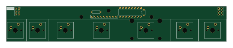 STM32
Type c
188 × 30 mm17 parts2LApache-2.02.9k