
Thiet lap PCB, Stackup va Design Rules

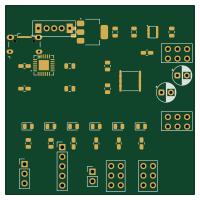
About the Thiet lap PCB, Stackup va Design Rules
Thiet lap PCB, Stackup va Design Rules is an open source PCB design by lengoctuong2005, published on GitHub. It is a 2-layer board measuring 50 × 50 mm, with 38 components from 24 distinct parts.
Other key parts include the AMS1117-3.3, LM2776, CP2102 and NE555. By type, the board carries 11 capacitors, 8 resistors, 7 connectors, 6 diodes, 4 ICs and 1 switch.
From the project
Tập hợp toàn bộ các bài thực hành và đồ án thiết kế PCB (KiCad) trong khóa học Thiết kế Mạch In / Vi Mạch.
Tập hợp toàn bộ các bài thực hành và đồ án thiết kế PCB (KiCad) trong khóa học Thiết kế Mạch In / Vi Mạch.
- CommonLibraries/: Thư viện linh kiện Footprint và Symbol tự tạo dùng chung. - Lab1/: Thiết kế Mạch Nguồn Cơ Bản (Schematic, PCB Layout, Báo cáo kỹ thuật). - Lab2/: Mạch Khuếch Đại / Cảm Biến & Sắp xếp linh kiện tiêu chuẩn. - Lab3/: Mạch Giao Tiếp & Chuyển Đổi Nguồn (Schematic, Routing 2 lớp, BOM, Báo cáo & Kiểm tra DRC/ERC). - Lab4/: Mạch Vi Điều Khiển / Ngoại Vi Mở Rộng. - Lab5/: Thiết Kế Mạch RF / Cao Tần & Layout Nâng Cao. - Lab6/: Tổng Hợp Thiết Kế Hoàn Chỉnh & Xuất File Gia Công…
Main components on the Thiet lap PCB, Stackup va Design Rules
Thiet lap PCB, Stackup va Design Rules bill of materials (BOM)
38 components, 24 distinct parts — part numbers from the project's BOM.
| Qty | Part | Footprint | Refs |
|---|---|---|---|
| 1 | AMS1117-3.3 | SOT-223-3_TabPin2 | U1 |
| 1 | LM2776 | SOT-23-6 | U2 |
| 1 | CP2102 | CP2102 | U3 |
| 1 | NE555 | SO-8_3.9x4.9mm_P1.27mm | U5 |
| 1 | Jumper 3 | PinHeader_1x03_P2.54mm_Vertical | J1 |
| 1 | jp5 | PinHeader_1x05_P2.54mm_Vertical | J3 |
| 1 | jp2 | PinHeader_1x02_P2.54mm_Vertical | J4 |
| 2 | Jumper 3 | Jumper 3 | J5, J6 |
| 2 | Connector_3x2 | Connector 3x2 | J7, J8 |
| 1 | ON/OFF SWITCH | SWITCH_ON_OFF | SW2 |
| 1 | Micro_USB | Micro_USB | USB1 |
| 1 | 5V | LED_0805_2012Metric | D1 |
| 1 | 3V3 | LED_0805_2012Metric | D2 |
| 1 | -VDD | LED_0805_2012Metric | D3 |
| 1 | 1Hz | LED_0805_2012Metric | D4 |
| 1 | RX1 | LED_0805_2012Metric | D5 |
| 1 | TX1 | LED_0805_2012Metric | D6 |
| 5 | 2.2uF | C_0805_2012Metric | C1, C3, C4, C5, C6 |
| 1 | 1uF | C_0805_2012Metric | C2 |
| 3 | 100nF | C_0805_2012Metric | C7, C8, C9 |
Show 4 more
| Qty | Part | Footprint | Refs |
|---|---|---|---|
| 2 | 10uF | CP_Radial_D5.0mm_P2.50mm | C10, C11 |
| 6 | 1k | R_0805_2012Metric | R1, R2, R3, R4, R5, R6 |
| 1 | 47k | R_0805_2012Metric | R7 |
| 1 | 100k | R_0805_2012Metric | R8 |
Thiet lap PCB, Stackup va Design Rules design files
The KiCad project lives in the lengoctuong2005/KiCad-PCB-Labs repository on GitHub; these links point at the commit this page was built from.
Thiet lap PCB, Stackup va Design Rules: common questions
How big is the Thiet lap PCB, Stackup va Design Rules?
The Thiet lap PCB, Stackup va Design Rules measures 50 × 50 mm, has 2 copper layers and is 1.6 mm thick.
How many components are on the Thiet lap PCB, Stackup va Design Rules?
38 components, from 24 distinct parts, with part numbers taken from the project's own BOM. The full bill of materials is listed on this page.
Where can I download the Thiet lap PCB, Stackup va Design Rules design files?
From the lengoctuong2005/KiCad-PCB-Labs repository on GitHub, which has the KiCad layout, the schematic and the BOM; the links under Design files point to each one.
Can I use the Thiet lap PCB, Stackup va Design Rules design in my own project?
The repository has no license, so all rights stay with lengoctuong2005. Use it as a reference, and ask the author before reusing the design.
More boards in KiCad-PCB-Labs
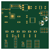
Lab 05: Placement - Bo tri linh kien tren
50 × 50 mm38 parts2LNo license1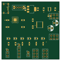
Lab8
50 × 50 mm38 parts2LNo license1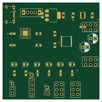
LAB7
50 × 50 mm38 parts2LNo license1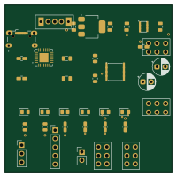
Lab 06: Routing - Ky thuat Di day Mach in tren
50 × 50 mm38 parts2LNo license1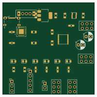
LAB3
50 × 50 mm38 parts2LNo license1
USB TypeC TP4056 Charger
22 × 34 mm18 parts2LNo license1