
PCB

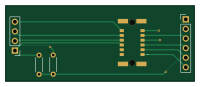
About the PCB
PCB is an open source PCB design by Lenka-12, published on GitHub. It is a 2-layer board measuring 50 × 20 mm, with 5 components from 5 distinct parts.
By type, the board carries 3 connectors and 2 resistors.
It belongs with the audio designs in this gallery.
From the project
A high-performance audio digitization system built around the STM32F7 microcontroller, featuring dual Delta-Sigma ADCs (PCM1808 and ADAU1978) and an integrated ADC for comprehensive audio capture.
A high-performance audio digitization system built around the STM32F7 microcontroller, featuring dual Delta-Sigma ADCs (PCM1808 and ADAU1978) and an integrated ADC for comprehensive audio capture.
This project implements a complete audio digitization pipeline that captures audio data through multiple ADCs and transmits it to a PC for MATLAB-based analysis.
The repository includes: - STEVAL-STWINMAV1 module adapter designs - Audio Digitisation Hardware based on PCM1862 (production pending) - ## 📊 Data Analysis
PCB bill of materials (BOM)
5 components, 5 distinct parts — part numbers from the project's BOM.
| Qty | Part | Footprint | Refs |
|---|---|---|---|
| 1 | M55-6001242R | M556001242R | J1 |
| 1 | IIS2 Conn_01x04_Pin | PinHeader_1x04_P2.54mm_Vertical | J2 |
| 1 | Conn_01x06_Pin | PinHeader_1x06_P2.54mm_Vertical | J3 |
| 1 | C25744 4.7k | R_Axial_DIN0204_L3.6mm_D1.6mm_P5.08mm_Horizontal | R1 |
| 1 | C25092 4.7k | R_Axial_DIN0204_L3.6mm_D1.6mm_P5.08mm_Horizontal | R2 |
PCB design files
The KiCad project lives in the Lenka-12/EEE4022S repository on GitHub; these links point at the commit this page was built from.
PCB: common questions
How big is the PCB?
The PCB measures 50 × 20 mm, has 2 copper layers and is 1.6 mm thick.
How many components are on the PCB?
5 components, from 5 distinct parts, with part numbers taken from the project's own BOM. The full bill of materials is listed on this page.
Where can I download the PCB design files?
From the Lenka-12/EEE4022S repository on GitHub, which has the KiCad layout, the schematic and the BOM; the links under Design files point to each one.
Can I use the PCB design in my own project?
The repository has no license, so all rights stay with Lenka-12. Use it as a reference, and ask the author before reusing the design.
More boards in EEE4022S
Similar boards
KLOR
GEIGEIGEIST
160.2 × 118.3 mm79 parts2LGPL-3.01.2k
ButtonsLEDs
shanteacontrols
390 × 37 mm82 parts2LApache-2.0956
USB
52 × 12.6 mm6 parts2LApache-2.0956
Pots
390 × 93 mm75 parts2LApache-2.0956
PicoGUS Hand386
polpo
29.2 × 75.2 mm43 parts4LGPL-2.0800
Snark barker
schlae
231.1 × 106.7 mm193 parts2LNo license687