
Netpuck

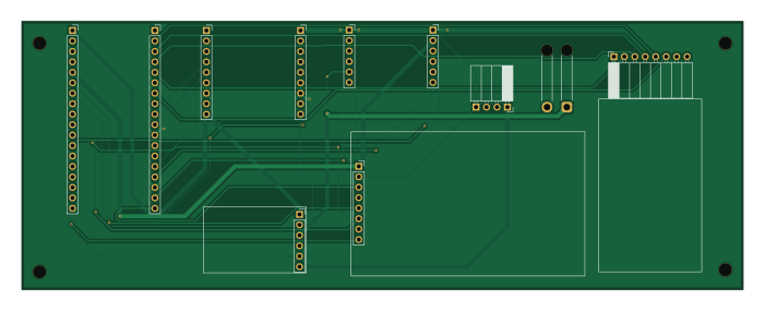
About the Netpuck PCB
Netpuck is an open source PCB design by leonampa, published on GitHub. It is a 2-layer board measuring 175 × 65 mm, with 11 components from 9 distinct parts.
It belongs with the iot & wireless and power & battery designs in this gallery.
From the project
[ARCHIVED] NetPuck 5G: A network auditing tool, using the ESP32-S3 and BW16 modules, that can scan for Access Point strength, and read details off an Ethernet connection, as a handheld, battery-operated device.
The NetPuck 5G is a handheld device, purpose-built to connect the worlds of software-driven network diagnostics and hardware-focused wireless analysis.
Made on Hack Club Blueprint 🚩- https://blueprint.hackclub.com/projects/13740
I needed a network auditing device. As a beginner IT Support Technician, I have a vast variety of tools for every job, but I've been lacking tools (and knowledge) regarding networking infrastructure. I've been making do with my phone and generic, no-brand WiFi strength scanning applications on my phone, but that is just not reliable for my purpose. I wanted to learn…
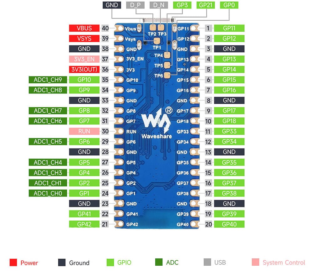
Netpuck bill of materials (BOM)
11 components, 9 distinct parts — part numbers from the project's BOM.
| Qty | Part | Footprint | Refs |
|---|---|---|---|
| 1 | Conn_01x02 | SolderWire-0.75sqmm_1x02_P4.8mm_D1.25mm_OD2.3mm_Relief | BTR1 |
| 2 | Conn_01x09_Socket | PinSocket_1x09_P2.54mm_Vertical | BW-16_L1, BW-16_R1 |
| 1 | ESP_L | PinSocket_1x18_P2.54mm_Vertical | ESP_L1 |
| 1 | Conn_01x18_Socket | PinSocket_1x18_P2.54mm_Vertical | ESP_R1 |
| 2 | Conn_01x06_Socket | PinSocket_1x06_P2.54mm_Vertical | ETH_L1, ETH_R1 |
| 1 | Conn_01x06_Socket | PinSocket_1x06_P2.54mm_Vertical | MH-CD42 |
| 1 | Conn_01x08_Socket | PinSocket_1x08_P2.54mm_Vertical | SCR1 |
| 1 | Conn_01x08_Socket | PinSocket_1x08_P2.54mm_Horizontal | STICK1 |
| 1 | Conn_01x04_Socket | PinSocket_1x04_P2.54mm_Horizontal | USB1 |
Netpuck design files
The KiCad project lives in the leonampa/netpuck repository on GitHub; these links point at the commit this page was built from.
- LayoutPCB/NetPuck5G.kicad_pcb
- SchematicPCB/NetPuck5G.kicad_sch
- BOMNetPuck 5G_BOM.csv
Netpuck: common questions
How big is the Netpuck PCB?
The Netpuck measures 175 × 65 mm, has 2 copper layers and is 1.6 mm thick.
How many components are on the Netpuck?
11 components, from 9 distinct parts, with part numbers taken from the project's own BOM. The full bill of materials is listed on this page.
Where can I download the Netpuck design files?
From the leonampa/netpuck repository on GitHub, which has the KiCad layout, the schematic and the BOM; the links under Design files point to each one.
Can I use the Netpuck design in my own project?
The repository has no license, so all rights stay with leonampa. Use it as a reference, and ask the author before reusing the design.
Similar boards

Stack chan
stack-chan
50 × 50 mm33 parts2LApache-2.01.7k
Display Carrier
AxxAxx
35.6 × 58.2 mm5 parts2LGPL-3.01.7k
ControllerCurrentShuntAddOn
stuartpittaway
26 × 16.9 mm9 parts2LCC-BY-NC-4.01.1k
Module 16S PassiveBalanceAddOn
61 × 74 mm86 parts2LCC-BY-NC-4.01.1k
TemperaturePCB PANEL
116 × 75.5 mm178 parts2LCC-BY-NC-4.01.1k
ProgrammingAdapter
10.5 × 83 mm3 parts2LCC-BY-NC-4.01.1k