
Back prototype

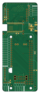
About the Back prototype PCB
Back prototype is an open source AVR/Arduino PCB design by libresmartphone, published on GitHub. It is a 2-layer board measuring 40 × 100 mm, with 65 components from 33 distinct parts.
Its main chip is the ATMEGA_HEADER, from the AVR/Arduino family. Other key parts include the OMAP3530DCBB, TPS65950BZXNR, SN74AVCA406LZXYR, USB3322C-GL and WG7210-00. By type, the board carries 21 capacitors, 12 jumpers, 10 connectors, 9 resistors, 6 ICs and 3 transistors.
It belongs with the audio and displays & leds designs in this gallery.
From the project
This page contains the software used in the open hardware smartphone (libresmartphone)
This is gamma version. It's WIP and is going to be sent to production soon (as soon as last TODOs are finished). You can already order this board, but it's possible the I2C GPIO expander pin mapping is going to change. Also, before ordering, please make sure the Gerber files are recent (if they're up-to-date after latest commits concerning PCB files) and regenerate them if necessary.
Main components on the Back prototype
Back prototype bill of materials (BOM)
65 components, 33 distinct parts — part numbers from the project's BOM.
| Qty | Part | Footprint | Refs |
|---|---|---|---|
| 1 | OMAP3530DCBB PI ZERO Texas Instruments Inc. | pi0outline | U1 |
| 1 | TPS65950BZXNR SIM800_BREAKOUT Texas Instruments Inc. | SIM800_BREAKOUT | U2 |
| 1 | SN74AVCA406LZXYR MCP23017 Texas Instruments Inc. | SOIC-28W_7.5x17.9mm_Pitch1.27mm | U3 |
| 1 | USB3322C-GL TP4056_BREAKOUT SMSC | TP4056_BREAKOUT | U4 |
| 1 | WG7210-00 RTC Jorjin Technologies Inc. | SOIC-8_3.9x4.9mm_Pitch1.27mm | U5 |
| 1 | DC_DC_BREAKOUT Texas Instruments Inc. | DC-DC-BREAKOUT | U6 |
| 2 | FDJ1027P IRLML6401 Fairchild Semiconductor | SOT-23_Handsoldering | Q1, Q2 |
| 1 | IRLML6401 | SOT-23_Handsoldering | Q4 |
| 1 | 32.768Hz | Crystal_SMD_G8-2pin_3.2x1.5mm_HandSoldering | Y1 |
| 1 | EXPANSION_LEFT | Pin_Header_Angled_1x13_Pitch2.54mm | P1 |
| 1 | EXPANSION_BOTTOM | Pin_Header_Angled_1x05_Pitch2.54mm | P2 |
| 1 | EXPANSION_TOP | Pin_Header_Angled_1x05_Pitch2.54mm | P3 |
| 2 | USB_A | USB_A | P4, P9 |
| 1 | AUDIO_CONN | Pin_Header_Straight_1x04_Pitch2.54mm | P5 |
| 1 | ATMEGA_HEADER | Pin_Header_Straight_1x06_Pitch2.54mm | P6 |
| 1 | EXPANSION_BOTTOM2 | Pin_Header_Angled_1x03_Pitch2.54mm | P7 |
| 1 | JST | JST_PH_S2B-PH-SM4-TB_02x2.00mm_Angled | P8 |
| 1 | CONN_01X08 | Pin_Header_Straight_1x08_Pitch2.54mm | P10 |
| 2 | JUMPER | GS2 | JP1, JP5 |
| 3 | JUMPER | GS2_SMALL | JP2, JP11, JP12 |
Show 13 more
| Qty | Part | Footprint | Refs |
|---|---|---|---|
| 1 | A0 | GS3_SMALL | JP3 |
| 1 | A1 | GS3_SMALL | JP4 |
| 2 | A2 | GS3_SMALL | JP6, JP8 |
| 3 | Jumper_NC_Small | GS2_SMALL | JP7, JP9, JP10 |
| 1 | SW_PUSH | SW_SPST_EVQPE1 | SW1 |
| 1 | ZHCS400TA SS14 Zetex | D_MiniMELF_Handsoldering | D1 |
| 1 | PGB0010603MR Led_RGB_CA_CC Littelfuse | RGB_5050 | D3 |
| 9 | 100nF | C_0805_HandSoldering | C1, C2, C5, C6, C8, C13, C14, C15 +1 |
| 3 | 100uF | CP_Tantalum_Case-B_EIA-3528-21_Hand | C3, C4, C7 |
| 6 | 10pF | C_0603_HandSoldering | C16, C17, C18, C19, C20, C21 |
| 3 | 33pF | C_0603_HandSoldering | C22, C23, C24 |
| 6 | 10K | R_0805_HandSoldering | R1, R2, R3, R4, R10, R11 |
| 3 | 1K | R_0805_HandSoldering | R5, R6, R7 |
Back prototype design files
The KiCad project lives in the libresmartphone/libresmartphone repository on GitHub; these links point at the commit this page was built from.
Back prototype: common questions
What microcontroller does the Back prototype use?
The Back prototype is built around the ATMEGA_HEADER, from the AVR/Arduino family.
How big is the Back prototype PCB?
The Back prototype measures 40 × 100 mm, has 2 copper layers and is 1.6 mm thick.
How many components are on the Back prototype?
65 components, from 33 distinct parts, with part numbers taken from the project's own BOM. The full bill of materials is listed on this page.
Where can I download the Back prototype design files?
From the libresmartphone/libresmartphone repository on GitHub, which has the KiCad layout and the BOM; the links under Design files point to each one.
Can I use the Back prototype design in my own project?
The repository has no license, so all rights stay with libresmartphone. Use it as a reference, and ask the author before reusing the design.
Can I test firmware for the Back prototype without the hardware?
Yes. HardLabs builds a simulation of the board from its netlist and BOM, so you can run and debug AVR/Arduino firmware against it before you order a PCB.
More boards in libresmartphone
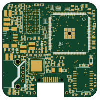
Woking
50 × 50 mm171 parts4LNo license33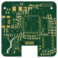
Eth
50 × 50 mm99 parts4LNo license33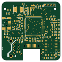
Mailbox
50 × 50 mm99 parts4LNo license33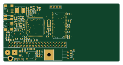
Calculator.test
100.4 × 50 mm90 parts4LNo license33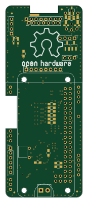 ESP8266
Front prototype
40 × 100 mm69 parts2LNo license33
.kicad
3 × 3 mm65 partsNo license33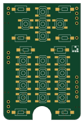
Keypad prototype
40 × 60 mm30 parts2LNo license33
Ssd1332 breakout
21 × 16.9 mm15 parts2LNo license33
Ltc2990 sensor
12.7 × 13.5 mm13 parts2LNo license33
Zerophone audio buffer
13.2 × 10.7 mm5 parts2LNo license33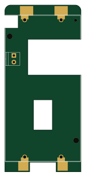
18650
40 × 88 mm3 parts2LNo license33
Similar boards
 AVR/Arduino
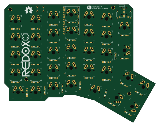
Redox keyboard
mattdibi
162.2 × 126.5 mm77 parts2LMIT2.0k AVR/Arduino
ModuleV450
stuartpittaway
30 × 61.4 mm39 parts2LCC-BY-NC-4.01.1k AVR/Arduino
V4
30 × 50 mm38 parts2LCC-BY-NC-4.01.1k AVR/Arduino
Discipline
coseyfannitutti
304.9 × 122.8 mm170 parts2LCC-BY-NC-4.01.0k AVR/Arduino
Megadesk
gcormier
41.7 × 32.2 mm23 parts2LGPL-3.0818 AVR/Arduino
Easyduino Atmega Nano
Hanqaqa
43.4 × 18 mm30 parts4LCERN-OHL-P-2.0746