
Sky130nm NFC

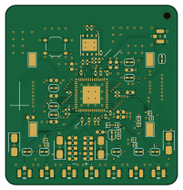
About the Sky130nm NFC PCB
Sky130nm NFC is an open source PCB design by morzack, published on GitHub. It is a 4-layer board measuring 50 × 52 mm, with 83 components from 19 distinct parts.
Other key parts include the W25Q32JVZP and Caravel_QFN. By type, the board carries 31 capacitors, 16 diodes, 12 resistors, 10 connectors, 4 test points and 2 ICs.
It belongs with the dev boards & breakouts designs in this gallery.
From the project
Design files for breakout and motherboard PCBs for Sky130 NFC chip designed in NCSU's Tapeout Course (spr2025)
submodules vendor in reference boards for tt06 and caravel.
most up-to-date caravel evaluation PCB at caravelboard/hardware/development/caravel-dev-v5-M.2` -- this contains details on FTDI module and flash memory for bringup of on-chip VexRiscv management CPU
1. make symbol for pinout (actual) 2. identify routing constaints for breakout 3. make block diagram of off-chip requirements for bringup 4. implement schematics for off-chip stuff 5. layout, etc
Main components on the Sky130nm NFC
Sky130nm NFC bill of materials (BOM)
83 components, 19 distinct parts.
| Qty | Part | Footprint | Refs |
|---|---|---|---|
| 1 | W25Q32JVZP | WSON-8-1EP_6x5mm_P1.27mm_EP3.4x4.3mm | U1 |
| 1 | Caravel_QFN | QFN-64-1EP_9x9mm_P0.5mm_EP7.65x7.65mm_SMALL_EPAD | U2 |
| 8 | U.FL-R-SMT-1_80_ | UFLRSMT180 | J1, J2, J3, J4, J5, J6, J7, J8 |
| 2 | DF40C-40DS-0.4V_51_ | DF40C40DS04V51 | J9, J10 |
| 5 | STITCHING_VIA_0p3mm | STITCHING_VIA_0p3mm | STITCHM1, STITCHM2, STITCHM3, STITCHM4, STITCHM5 |
| 1 | SW_Push | SW_Push_1P1T_XKB_TS-1187A | SW1 |
| 4 | 5019 TestPoint_Alt | TestPoint_Keystone_5019_Minature | TP1, TP2, TP3, TP4 |
| 12 | PESD3V3S1UL | D_SOD-882 | D1, D2, D3, D4, D5, D6, D7, D8 +4 |
| 4 | SMAJ10CA | D_SMA | D9, D12, D13, D16 |
| 2 | L0 | L_0603_1608Metric_Pad1.05x0.95mm_HandSolder | L1, L2 |
| 13 | 0.1uf | C_0402_1005Metric | C1, C3, C7, C8, C9, C12, C13, C15 +5 |
| 12 | C_1u_0603_50V | C_0603_1608Metric | C2, C4, C5, C6, C10, C11, C14, C17 +4 |
| 2 | C0 | C_0603_1608Metric_Pad1.08x0.95mm_HandSolder | C26, C27 |
| 2 | CA | C_0603_1608Metric_Pad1.08x0.95mm_HandSolder | C28, C31 |
| 2 | CB | C_0603_1608Metric_Pad1.08x0.95mm_HandSolder | C29, C30 |
| 3 | 10k | R_0402_1005Metric | R1, R3, R4 |
| 3 | 0 | R_0402_1005Metric | R2, R5, R6 |
| 4 | 50 | R_0402_1005Metric | R7, R8, R9, R10 |
| 2 | Rq | R_0603_1608Metric_Pad0.98x0.95mm_HandSolder | R11, R12 |
Sky130nm NFC design files
The KiCad project lives in the morzack/ece592-nfc-caravan-pcbs repository on GitHub; these links point at the commit this page was built from.
Sky130nm NFC: common questions
How big is the Sky130nm NFC PCB?
The Sky130nm NFC measures 50 × 52 mm, has 4 copper layers and is 1.61668 mm thick.
How many components are on the Sky130nm NFC?
83 components, from 19 distinct parts. The full bill of materials is listed on this page.
Where can I download the Sky130nm NFC design files?
From the morzack/ece592-nfc-caravan-pcbs repository on GitHub, which has the KiCad layout and the schematic; the links under Design files point to each one.
Can I use the Sky130nm NFC design in my own project?
The repository has no license, so all rights stay with morzack. Use it as a reference, and ask the author before reusing the design.
More boards in ece592-nfc-caravan-pcbs
Similar boards
88 Pin Vag Breakout
rusefi
142 × 58 mm91 parts2LGPL-3.01.2k
134pin 7-967288-1
139.7 × 73.7 mm38 parts2LGPL-3.01.2k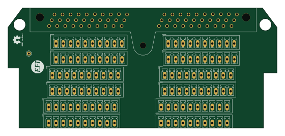
Breakout 60pin EEC-IV
139.7 × 62.2 mm15 parts2LGPL-3.01.2k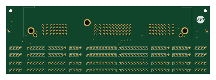
Breakout 112pin Connector
174 × 58 mm39 parts2LGPL-3.01.2k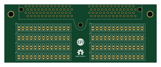
Eecv breakout
140.8 × 53.7 mm9 parts4LGPL-3.01.2k
Rj45 breakout
rene-dev
15.2 × 53.8 mm3 parts2LGPL-3.0979