
Stm32f446re breakout substrate

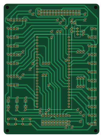
About the Stm32f446re breakout substrate
Stm32f446re breakout substrate is an open source STM32 PCB design by MUNAKATA-EPC, published on GitHub. It is a 2-layer board measuring 83.8 × 114.2 mm, with 84 components from 56 distinct parts.
Its main chip is the STM32F446RE, from the STM32 family. By type, the board carries 71 connectors, 3 diodes, 3 capacitors, 3 resistors, 2 ICs and 2 switches.
It belongs with the dev boards & breakouts designs in this gallery.
From the project
チームメンバー間の仲は良好です
Munako_Amateras 2026年度:サッカーライトウェイトリーグ出場 2027年度:サッカーオープンリーグ出場予定
Stm32f446re breakout substrate bill of materials (BOM)
84 components, 56 distinct parts.
| Qty | Part | Footprint | Refs |
|---|---|---|---|
| 1 | ~ | STM32F446RE | U1 |
| 1 | ~ | TO220F | U3 |
| 1 | Conn_01x07_Socket | PinSocket_1x07_P2.54mm_Vertical | J1 |
| 7 | Conn_01x04_Socket | PinSocket_1x04_P2.54mm_Vertical | J2, J3, J4, J5, J6, J7, J8 |
| 11 | Conn_01x03_Socket | PinSocket_1x03_P2.54mm_Vertical | J9, J10, J11, J12, J13, J14, J15, J16 +3 |
| 3 | Conn_01x10_Socket | PinSocket_1x10_P2.54mm_Vertical | J18, J19, J21 |
| 1 | Conn_01x02_Socket | PinSocket_1x02_P2.54mm_Vertical | J22 |
| 1 | J1_B | PinSocket_1x01_P2.54mm_Vertical | J24 |
| 1 | J2_B | PinSocket_1x01_P2.54mm_Vertical | J25 |
| 1 | J3_B | PinSocket_1x01_P2.54mm_Vertical | J26 |
| 1 | J1_A | PinSocket_1x01_P2.54mm_Vertical | J27 |
| 1 | J2_A | PinSocket_1x01_P2.54mm_Vertical | J28 |
| 1 | J3_A | PinSocket_1x01_P2.54mm_Vertical | J29 |
| 1 | J4_B | PinSocket_1x01_P2.54mm_Vertical | J30 |
| 1 | J5_B | PinSocket_1x01_P2.54mm_Vertical | J31 |
| 1 | J4_A | PinSocket_1x01_P2.54mm_Vertical | J32 |
| 1 | J5_A | PinSocket_1x01_P2.54mm_Vertical | J33 |
| 1 | J6_B | PinSocket_1x01_P2.54mm_Vertical | J34 |
| 1 | J7_B | PinSocket_1x01_P2.54mm_Vertical | J35 |
| 1 | J6_A | PinSocket_1x01_P2.54mm_Vertical | J36 |
Show 36 more
| Qty | Part | Footprint | Refs |
|---|---|---|---|
| 1 | J7_A | PinSocket_1x01_P2.54mm_Vertical | J37 |
| 1 | J9_B | PinSocket_1x01_P2.54mm_Vertical | J38 |
| 1 | J8_B | PinSocket_1x01_P2.54mm_Vertical | J39 |
| 1 | J8_A | PinSocket_1x01_P2.54mm_Vertical | J40 |
| 1 | J9_A | PinSocket_1x01_P2.54mm_Vertical | J41 |
| 1 | J10_B | PinSocket_1x01_P2.54mm_Vertical | J42 |
| 1 | J10_A | PinSocket_1x01_P2.54mm_Vertical | J43 |
| 1 | J11_B | PinSocket_1x01_P2.54mm_Vertical | J44 |
| 1 | J11_A | PinSocket_1x01_P2.54mm_Vertical | J45 |
| 1 | J12_B | PinSocket_1x01_P2.54mm_Vertical | J46 |
| 1 | J12_A | PinSocket_1x01_P2.54mm_Vertical | J47 |
| 1 | J13_B | PinSocket_1x01_P2.54mm_Vertical | J48 |
| 1 | J13_A | PinSocket_1x01_P2.54mm_Vertical | J49 |
| 1 | J14_B | PinSocket_1x01_P2.54mm_Vertical | J50 |
| 1 | J14_A | PinSocket_1x01_P2.54mm_Vertical | J51 |
| 1 | J16_B | PinSocket_1x01_P2.54mm_Vertical | J52 |
| 1 | J15_B | PinSocket_1x01_P2.54mm_Vertical | J53 |
| 1 | J15_A | PinSocket_1x01_P2.54mm_Vertical | J54 |
| 1 | J16_A | PinSocket_1x01_P2.54mm_Vertical | J55 |
| 1 | J17_B | PinSocket_1x01_P2.54mm_Vertical | J56 |
| 1 | J17_A | PinSocket_1x01_P2.54mm_Vertical | J57 |
| 2 | J18_A | PinSocket_1x01_P2.54mm_Vertical | J58, J63 |
| 2 | J19_A | PinSocket_1x01_P2.54mm_Vertical | J59, J62 |
| 2 | J20_A | PinSocket_1x01_P2.54mm_Vertical | J60, J61 |
| 2 | Conn_01x15_Socket | PinSocket_1x15_P2.54mm_Vertical | J64, J65 |
| 1 | J21_A | PinSocket_1x01_P2.54mm_Vertical | J66 |
| 1 | J21_B | PinSocket_1x01_P2.54mm_Vertical | J67 |
| 1 | J22_B | PinSocket_1x01_P2.54mm_Vertical | J68 |
| 1 | J22_A | PinSocket_1x01_P2.54mm_Vertical | J69 |
| 1 | J23_B | PinSocket_1x01_P2.54mm_Vertical | J70 |
| 1 | J23_A | PinSocket_1x01_P2.54mm_Vertical | J71 |
| 2 | SW_Push | SW_PUSH_6mm_H5mm | SW1, SW2 |
| 3 | LED | PinSocket_1x02_P2.54mm_Vertical | D1, D2, D3 |
| 2 | C | PinSocket_1x02_P2.54mm_Vertical | C1, C2 |
| 1 | C_Polarized | PinSocket_1x02_P2.54mm_Vertical | C3 |
| 3 | R | PinSocket_1x02_P2.54mm_Vertical | R1, R2, R3 |
Stm32f446re breakout substrate design files
The KiCad project lives in the MUNAKATA-EPC/Amateras repository on GitHub; these links point at the commit this page was built from.
Stm32f446re breakout substrate: common questions
What microcontroller does the Stm32f446re breakout substrate use?
The Stm32f446re breakout substrate is built around the STM32F446RE, from the STM32 family.
How big is the Stm32f446re breakout substrate?
The Stm32f446re breakout substrate measures 83.8 × 114.2 mm, has 2 copper layers and is 1.6 mm thick.
How many components are on the Stm32f446re breakout substrate?
84 components, from 56 distinct parts. The full bill of materials is listed on this page.
Where can I download the Stm32f446re breakout substrate design files?
From the MUNAKATA-EPC/Amateras repository on GitHub, which has the KiCad layout and the schematic; the links under Design files point to each one.
Can I use the Stm32f446re breakout substrate design in my own project?
The repository has no license, so all rights stay with MUNAKATA-EPC. Use it as a reference, and ask the author before reusing the design.
Can I test firmware for the Stm32f446re breakout substrate without the hardware?
Yes. HardLabs builds a simulation of the board from its netlist and BOM, so you can run and debug STM32 firmware against it before you order a PCB.
More boards in Amateras
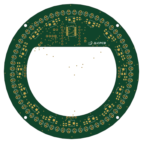
LINE Main
119.4 × 119.4 mm137 parts2LNo license1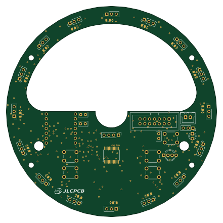
IR board syuuseibann
110 × 110 mm64 parts2LNo license1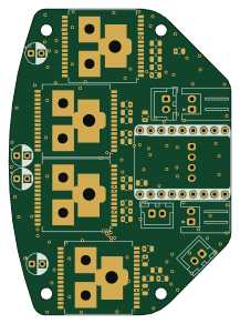 RP2040/RP2350
Drive
53 × 72.8 mm39 parts4LNo license1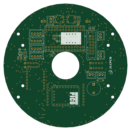 RP2040/RP2350
Main board
110 × 110 mm35 parts2LNo license1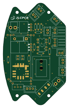
電源基板
55.1 × 90 mm34 parts2LNo license1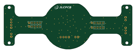
Highway
118.8 × 42.4 mm10 parts2LNo license1
Similar boards
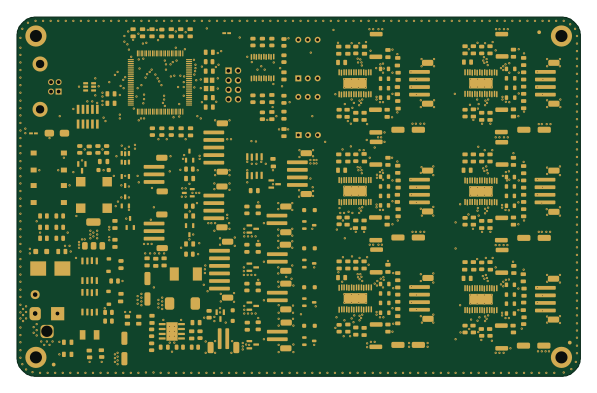 STM32
LumenPnP Motherboard
opulo-inc
149 × 95 mm296 parts4LCC-BY-SA-4.03.7k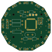 STM32
Base
google
52.3 × 52.3 mm36 parts2LApache-2.02.9k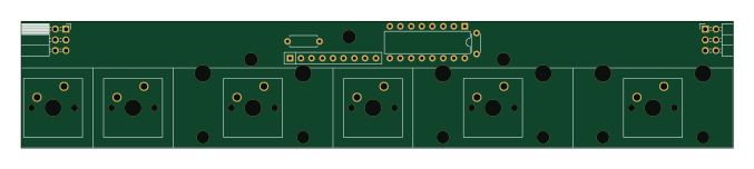 STM32
Type g
169 × 30 mm24 parts2LApache-2.02.9k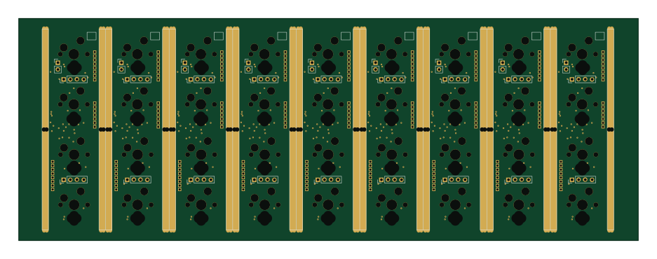 STM32
Main panel
234 × 84 mm26 parts4LApache-2.02.9k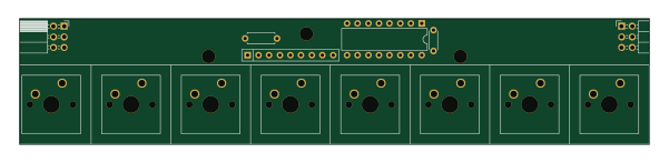 STM32
Type a
150 × 30 mm14 parts2LApache-2.02.9k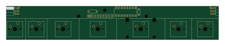 STM32
Type c
188 × 30 mm17 parts2LApache-2.02.9k