
FutekTestBedCircuit

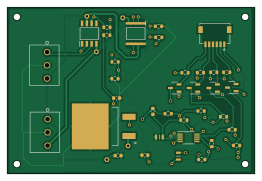
About the FutekTestBedCircuit PCB
FutekTestBedCircuit is an open source PCB design by neurobionics, published on GitHub. It is a 2-layer board measuring 65.5 × 44 mm, with 35 components from 12 distinct parts.
Other key parts include the OP07, L7805 and ADS1115IDGS. By type, the board carries 18 resistors, 4 ICs, 4 transistors, 4 capacitors, 3 connectors and 2 inductors.
From the project
- Circuit Layout (see KiCAD Schema File and IMG) - The KiCAD Schematic (see KiCAD Schema File) - The KiCAD PCB Design - JLC PCB Account [For Ordering] - reach out to @Japmanjeet Singh Gill for login details - BOM and CPL Files (See FinalOrderingPackage Folder)
- Circuit Layout (see KiCAD Schema File and IMG) - The KiCAD Schematic (see KiCAD Schema File) - The KiCAD PCB Design - JLC PCB Account [For Ordering] - reach out to @Japmanjeet Singh Gill for login details - BOM and CPL Files (See FinalOrderingPackage Folder)
*Note- if cannot login to JLC PCB Account, see the image " JLCPCB COMPONENT PNs " and copy PNs from that file. Note - connectors J1, J2, J3 not placed in the production files. - J1 and J2 are through-hole placement and J3 has part shortages in china
Main components on the FutekTestBedCircuit
FutekTestBedCircuit bill of materials (BOM)
35 components, 12 distinct parts.
| Qty | Part | Footprint | Refs |
|---|---|---|---|
| 2 | OP07 | SOIC127P600X175-8N | U1, U2 |
| 1 | L7805 | D2PAK-STB35NF10T4 | U3 |
| 1 | ADS1115IDGS | VSSOP-10_3x3mm_P0.5mm | U4 |
| 4 | BSS138 | SOT-23-3 | Q1, Q2, Q3, Q4,3,2,1 |
| 2 | Conn_01x03 | CONN_1984620_PXC | J1, J2 |
| 1 | Conn_01x06 | MOLEX_2035580607 | J3 |
| 2 | FerriteBead | BLM21AG102BH1J | FB2, FB3 |
| 1 | 0.1u | C_0603_1608Metric | C1 |
| 2 | 1u | C_0603_1608Metric | C2, C3 |
| 1 | 0.33u | C_0603_1608Metric | C4 |
| 16 | 10K | R_0603_1608Metric | R1, R2, R4, R6, R7, R8, R9, R10 +8 |
| 2 | 0 | R_0603_1608Metric | R3, R5 |
FutekTestBedCircuit design files
The KiCad project lives in the neurobionics/FutekTestBedCircuit repository on GitHub; these links point at the commit this page was built from.
FutekTestBedCircuit: common questions
How big is the FutekTestBedCircuit PCB?
The FutekTestBedCircuit measures 65.5 × 44 mm, has 2 copper layers and is 1.62 mm thick.
How many components are on the FutekTestBedCircuit?
35 components, from 12 distinct parts. The full bill of materials is listed on this page.
Where can I download the FutekTestBedCircuit design files?
From the neurobionics/FutekTestBedCircuit repository on GitHub, which has the KiCad layout and the schematic; the links under Design files point to each one.
Can I use the FutekTestBedCircuit design in my own project?
The repository has no license, so all rights stay with neurobionics. Use it as a reference, and ask the author before reusing the design.