
-fpga hash accelerator

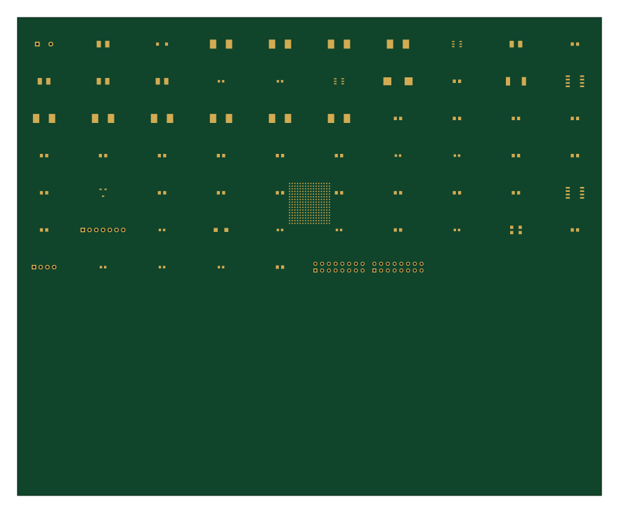
About the -fpga hash accelerator PCB
-fpga hash accelerator is an open source PCB design by Nivi77, published on GitHub under the MIT license. It is a 4-layer board measuring 220 × 180 mm, with 56 components from 56 distinct parts.
Other key parts include the Buck 12V->3.3V (3A), Buck 3.3V->1.0V (20A, VCORE), Shunt current monitor, LDO 3.3V->2.5V (VCCAUX) and SPI Flash (bitstream). By type, the board carries 6 ICs, 5 connectors, 3 inductors, 1 crystal, 1 fuse and 1 switch.
It belongs with the power & battery and dev boards & breakouts designs in this gallery.
From the project
A carrier board for an FPGA-based hashing accelerator, with the emphasis on the part that actually differentiates this from a generic dev board: a power delivery network (PDN) sized for sudden, large current transients on the FPGA core rail, which is the defining challenge of any
A carrier board for an FPGA-based hashing accelerator, with the emphasis on the part that actually differentiates this from a generic dev board: a power delivery network (PDN) sized for sudden, large current transients on the FPGA core rail, which is the defining challenge of any dense digital-logic accelerator (hashing, mining, ML inference, etc.) — large blocks of logic can switch simultaneously and pull amp-scale current steps in nanoseconds. Built in KiCad 8.
Main components on the -fpga hash accelerator
-fpga hash accelerator bill of materials (BOM)
56 components, 56 distinct parts — part numbers from the project's BOM.
| Qty | Part | Footprint | Refs |
|---|---|---|---|
| 1 | FPGA (generic BGA256 - substitute real device pinout) | U1_FPGA_BGA256 | U1 |
| 1 | Buck 12V->3.3V (3A) | U3_BUCK6 | U3 |
| 1 | Buck 3.3V->1.0V (20A, VCORE) | U4_BUCK6 | U4 |
| 1 | Shunt current monitor | U5_CURMON8 | U5 |
| 1 | LDO 3.3V->2.5V (VCCAUX) | U6_LDO3 | U6 |
| 1 | SPI Flash (bitstream) | U7_SPIFLASH8 | U7 |
| 1 | 50MHz oscillator | Y1_OSC3 | Y1 |
| 1 | 12V DC Input | J1_CONN2 | J1 |
| 1 | JTAG header | J2_HDR7 | J2 |
| 1 | I2C monitor header | J3_HDR4 | J3 |
| 1 | GPIO header A (GPIO0-15) | J4_HDR16 | J4 |
| 1 | GPIO header B (GPIO16-31) | J5_HDR16 | J5 |
| 1 | 100uF (bulk in) | CB1_C | CB1 |
| 1 | 100uF (bulk in) | CB2_C | CB2 |
| 1 | 100uF (bulk in) | CB3_C | CB3 |
| 1 | 100uF (bulk in) | CB4_C | CB4 |
| 1 | 220uF polymer (bulk, spike buffer) | CBC1_C | CBC1 |
| 1 | 220uF polymer (bulk, spike buffer) | CBC2_C | CBC2 |
| 1 | 220uF polymer (bulk, spike buffer) | CBC3_C | CBC3 |
| 1 | 220uF polymer (bulk, spike buffer) | CBC4_C | CBC4 |
Show 36 more
| Qty | Part | Footprint | Refs |
|---|---|---|---|
| 1 | 220uF polymer (bulk, spike buffer) | CBC5_C | CBC5 |
| 1 | 220uF polymer (bulk, spike buffer) | CBC6_C | CBC6 |
| 1 | 10nF (bootstrap) | CBT1_C | CBT1 |
| 1 | 10nF (bootstrap) | CBT2_C | CBT2 |
| 1 | 100nF (HF decouple, at FPGA) | CDC1_C | CDC1 |
| 1 | 100nF (HF decouple, at FPGA) | CDC2_C | CDC2 |
| 1 | 100nF (HF decouple, at FPGA) | CDC3_C | CDC3 |
| 1 | 100nF (HF decouple, at FPGA) | CDC4_C | CDC4 |
| 1 | 100nF (HF decouple, at FPGA) | CDC5_C | CDC5 |
| 1 | 100nF (HF decouple, at FPGA) | CDC6_C | CDC6 |
| 1 | 100nF (HF decouple, at FPGA) | CDC7_C | CDC7 |
| 1 | 100nF (HF decouple, at FPGA) | CDC8_C | CDC8 |
| 1 | 100nF (HF decouple, at FPGA) | CDC9_C | CDC9 |
| 1 | 100nF (HF decouple, at FPGA) | CDC10_C | CDC10 |
| 1 | 100nF | CFL1_C | CFL1 |
| 1 | 100nF | CIO1_C | CIO1 |
| 1 | 100nF | CIO2_C | CIO2 |
| 1 | 100nF | CIO3_C | CIO3 |
| 1 | 100nF | CIO4_C | CIO4 |
| 1 | 1uF | CLDO1_C | CLDO1 |
| 1 | 10uF | CLDO2_C | CLDO2 |
| 1 | 22uF | CO1_1_C | CO1_1 |
| 1 | 22uF | CO1_2_C | CO1_2 |
| 1 | 22uF | CO1_3_C | CO1_3 |
| 1 | 1uF | CPLL1_C | CPLL1 |
| 1 | 100nF | CPLL2_C | CPLL2 |
| 1 | 3A Polyfuse | F1_R | F1 |
| 1 | 100k | RF1A_R | RF1A |
| 1 | 45.3k | RF1B_R | RF1B |
| 1 | 66.7k | RF2A_R | RF2A |
| 1 | 100k | RF2B_R | RF2B |
| 1 | PROGRAM button | SW1_CONN2 | SW1 |
| 1 | TVS 18V (surge) | D1_D | D1 |
| 1 | Ferrite bead (PLL filter) | FB1PLL_L | FB1PLL |
| 1 | 4.7uH | L1_L | L1 |
| 1 | 1.0uH (power inductor) | L2_L | L2 |
-fpga hash accelerator design files
The KiCad project lives in the Nivi77/-fpga-hash-accelerator repository on GitHub; these links point at the commit this page was built from.
-fpga hash accelerator: common questions
How big is the -fpga hash accelerator PCB?
The -fpga hash accelerator measures 220 × 180 mm, has 4 copper layers and is 1.6 mm thick.
How many components are on the -fpga hash accelerator?
56 components, from 56 distinct parts, with part numbers taken from the project's own BOM. The full bill of materials is listed on this page.
Where can I download the -fpga hash accelerator design files?
From the Nivi77/-fpga-hash-accelerator repository on GitHub, which has the KiCad layout, the schematic and the BOM; the links under Design files point to each one.
Can I use the -fpga hash accelerator design in my own project?
Yes, under the terms of its MIT license, which Nivi77 chose for the repository.
Similar boards

Stack chan
stack-chan
50 × 50 mm33 parts2LApache-2.01.7k
Display Carrier
AxxAxx
35.6 × 58.2 mm5 parts2LGPL-3.01.7k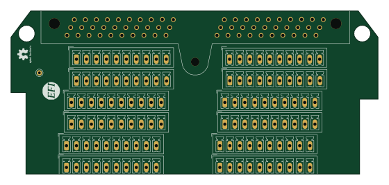
Breakout 60pin EEC-IV
rusefi
139.7 × 62.2 mm15 parts2LGPL-3.01.2k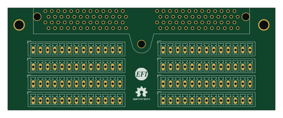
Eecv breakout
140.8 × 53.7 mm9 parts4LGPL-3.01.2k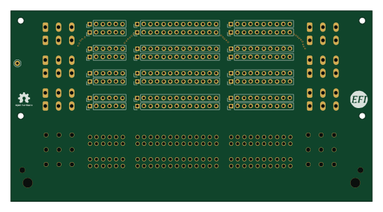
134pin 7-967288-1
139.7 × 73.7 mm38 parts2LGPL-3.01.2k
Breakout 112pin Connector
174 × 58 mm39 parts2LGPL-3.01.2k