
PCB BackDesign

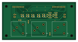
About the PCB BackDesign
PCB BackDesign is an open source PCB design by NUbots, published on GitHub. It is a 2-layer board measuring 62.5 × 32 mm, with 28 components from 14 distinct parts.
By type, the board carries 11 resistors, 7 diodes, 4 connectors, 3 switches and 3 capacitors.
It belongs with the robotics & motion designs in this gallery.
From the project
Hardware used by the NUbots team.
An alternative for future revisions is the 5501M series which has a longer travel of about 1 mm -- the datasheet is somewhat ambiguous. It can even have an embedded LED which can be wired to the second arm of a SPDT -- labelled NC in the datasheet -- and can be used to signify when the button is pressed as a form of visual feedback. However, compared to the KS11R2xCQD, it has a much taller profile which would mean that the PCB would need to be recessed further back into the torso.
PCB BackDesign bill of materials (BOM)
28 components, 14 distinct parts.
| Qty | Part | Footprint | Refs |
|---|---|---|---|
| 1 | Molex Picoblade 0530470810 | Molex_PicoBlade_53047-0810_1x08_P1.25mm_Vertical | J1 |
| 1 | Molex Picoblade 0530470910 | Molex_PicoBlade_53047-0910_1x09_P1.25mm_Vertical | J2 |
| 2 | B2B-PH-K-S | JST_PH_B2B-PH-K_1x02_P2.00mm_Vertical | J3, J4 |
| 1 | KS11R23CQD (red) | KS11_CNK | SW1 |
| 1 | KS11R22CQD (black) | KS11_CNK | SW2 |
| 1 | KS11R27CQD (blue) | KS11_CNK | SW3 |
| 2 | LED (yellow-green) 5988060107F | LED_0603_1608Metric | D1, D2 |
| 1 | LED (red) 5988010107F | LED_0603_1608Metric | D3 |
| 1 | LED (blue) 5988091107F | LED_0603_1608Metric | D4 |
| 1 | LED (green) 5988070107F | LED_0603_1608Metric | D5 |
| 2 | EAST1616RGBB2 | LED_LiteOn_LTST-C19HE1WT | D6, D7 |
| 3 | 100nF | C_0603_1608Metric | C1, C2, C3 |
| 5 | 470Ω | R_0603_1608Metric | R1, R2, R3, R8, R10 |
| 6 | 240Ω | R_0603_1608Metric | R4, R5, R6, R7, R9, R11 |
PCB BackDesign design files
The KiCad project lives in the NUbots/NUware repository on GitHub; these links point at the commit this page was built from.
PCB BackDesign: common questions
How big is the PCB BackDesign?
The PCB BackDesign measures 62.5 × 32 mm, has 2 copper layers and is 1.6 mm thick.
How many components are on the PCB BackDesign?
28 components, from 14 distinct parts. The full bill of materials is listed on this page.
Where can I download the PCB BackDesign design files?
From the NUbots/NUware repository on GitHub, which has the KiCad layout and the schematic; the links under Design files point to each one.
Can I use the PCB BackDesign design in my own project?
The repository has no license, so all rights stay with NUbots. Use it as a reference, and ask the author before reusing the design.
More boards in NUware
Similar boards
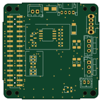
Stack chan
stack-chan
50 × 50 mm33 parts2LApache-2.01.7k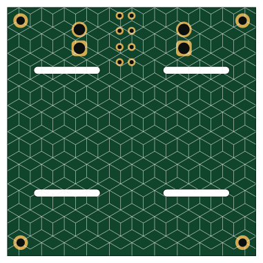
Cube batteryboard
willem-pennings
95 × 95 mm4 parts2LGPL-3.01.1k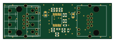
11ua
rene-dev
57.3 × 19 mm26 parts2LGPL-3.0979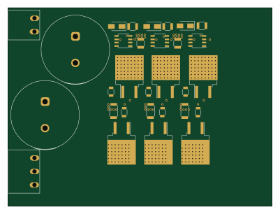
Trollerv2
100 × 75 mm33 parts4LGPL-3.0979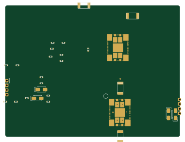
Powerstep
95.2 × 71.5 mm28 parts4LGPL-3.0979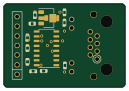
Diff driver
32 × 22 mm14 parts2LGPL-3.0979