
Quanta75 RP2040Stamp JLCPCBAoptimized

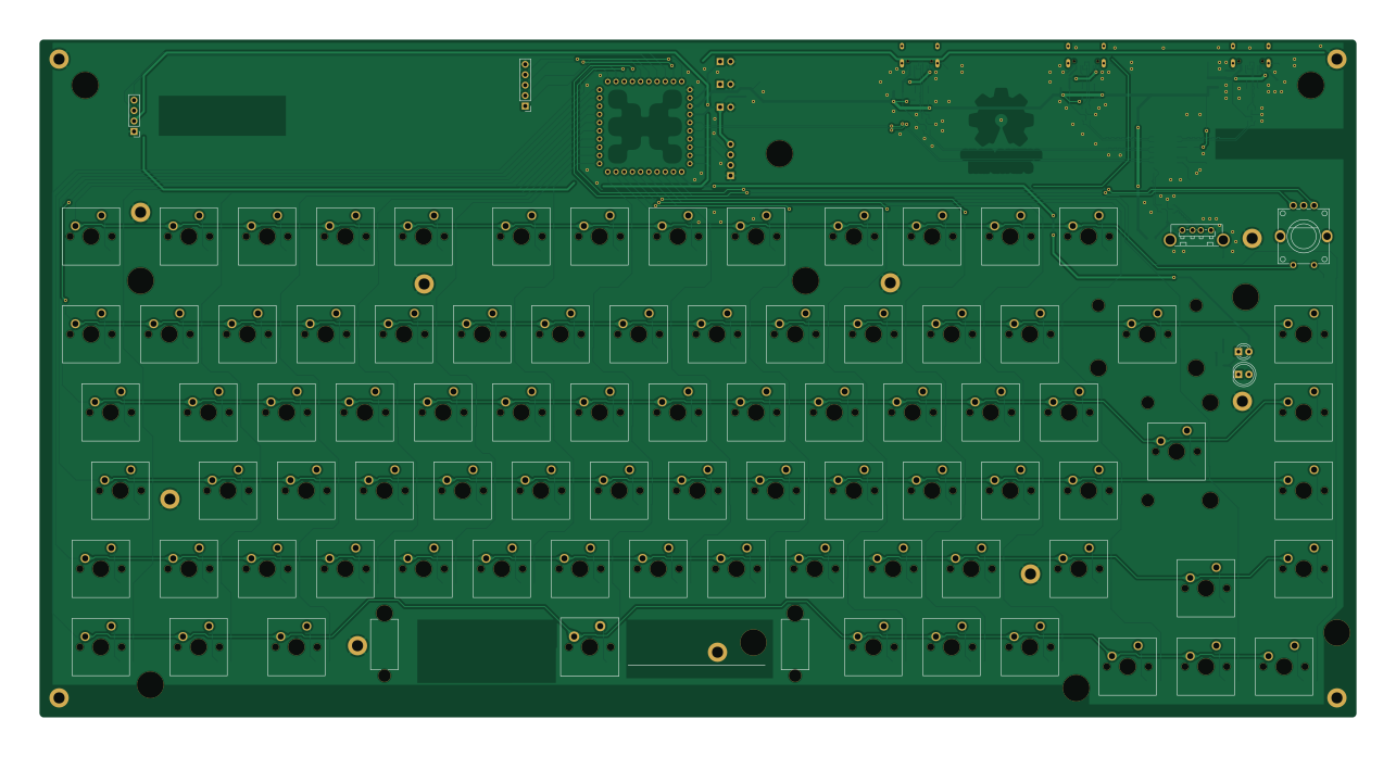
About the Quanta75 RP2040Stamp JLCPCBAoptimized PCB
Quanta75 RP2040Stamp JLCPCBAoptimized is an open source RP2040/RP2350 PCB design by obsilab, published on GitHub under the CERN-OHL-P-2.0 license. It is a 2-layer board measuring 320.7 × 165.1 mm, with 217 components from 33 distinct parts.
Its main chip is the RP2040_Stamp, from the RP2040/RP2350 family. Other key parts include the SL2.1A. By type, the board carries 88 diodes, 82 switches, 15 resistors, 10 connectors, 9 inductors and 9 capacitors.
It belongs with the keyboards designs in this gallery.
From the project
Custom 75% keyboard (currently ISO layout only)
All of them are using SMD components but no smaller than 0603 and on hand-solderable pads (a complete through-hole PCB could be coming next 👀). A PCB assembly service is still recommended.
rmkfirmware WIP_ RMK is a keyboard firmware written in Rust, inspired by QMK or KMK. Originally built for the Quanta.

Main components on the Quanta75 RP2040Stamp JLCPCBAoptimized
Quanta75 RP2040Stamp JLCPCBAoptimized bill of materials (BOM)
217 components, 33 distinct parts.
| Qty | Part | Footprint | Refs |
|---|---|---|---|
| 1 | RP2040_Stamp | RP2040_Stamp_THT | U1 |
| 1 | SL2.1A CoreChips(和芯润德) | SOP-16_L10.0-W3.9-P1.27-LS6.0-BL | U2 |
| 3 | USB_C_Receptacle_USB2.0 | USB-C-SMD_G-SWITCH_GT-USB-7010EN | J1, J7, J9 |
| 1 | Conn_01x02_Socket VBUS 5V | PinHeader_1x02_P2.54mm_Vertical | J2 |
| 1 | Conn_01x02_Socket 3V3 | PinHeader_1x02_P2.54mm_Vertical | J3 |
| 1 | Conn_01x02_Socket VBAT | PinHeader_1x02_P2.54mm_Vertical | J4 |
| 1 | Conn_01x04_Socket SWD | PinHeader_1x04_P2.54mm_Vertical | J5 |
| 1 | USB_A_Receptacle_UBS2.0 | USB-A-TH_KH-AF180ZJ-13.7 | J6 |
| 1 | Conn_01x04_Socket I2C display | PinHeader_1x04_P2.54mm_Vertical | J8 |
| 1 | Conn_01x05_Socket GPIOs | PinHeader_1x05_P2.54mm_Vertical | J10 |
| 1 | DIODE | D_SOD-123 | RED1 |
| 1 | RotaryEncoder_Switch | SW-TH_PEC12R-4120F-S0012 | RESW1 |
| 72 | SW_Push | SW_Cherry_MX_1.00u_PCB | SW1, SW2, SW3, SW4, SW5, SW6, SW7, SW8 +64 |
| 1 | SW_Push | SW_Cherry_MX_2.00u_PCB | SW27 |
| 1 | SW_Push | SW_Cherry_MX_1.50u_PCB | SW29 |
| 1 | SW_Push | SW_Cherry_MX_ISOEnter_PCB | SW42 |
| 2 | SW_Push | SW_Cherry_MX_1.75u_PCB | SW44, SW70 |
| 4 | SW_Push | SW_Cherry_MX_1.25u_PCB | SW58, SW73, SW74, SW75 |
| 1 | SW_Push | SW_Cherry_MX_PCB_6.25u | SW76 |
| 82 | DIODE | D_SOD-123 | D1, D2, D3, D4, D5, D6, D7, D8 +74 |
Show 13 more
| Qty | Part | Footprint | Refs |
|---|---|---|---|
| 4 | USBLC6-2SC6 | SOT-23-6_Handsoldering | D83, D84, D85, D86 |
| 1 | Amber LED | LED_D5.0mm_Clear | D87 |
| 1 | Amber LED | LED_D3.0mm_Clear | D88 |
| 4 | 600R | Ferrite_0805_2012Metric | FB1, FB2, FB3, FB8 |
| 2 | 100R 800mA | Ferrite_0805_2012Metric_Pad1.05x1.20mm_BigPads | FB4, FB9 |
| 3 | 600R 500mA | Ferrite_0805_2012Metric | FB5, FB6, FB7 |
| 3 | 10uF | C_0603_1608Metric_Pad1.08x0.95mm_HandSolder | C1, C2, C4 |
| 2 | 100nF | C_0603_1608Metric_Pad1.08x0.95mm_HandSolder | C3, C7 |
| 4 | 100uF | C_1206_3216Metric_Pad1.33x1.80mm_HandSolder | C5, C6, C8, C9 |
| 5 | 120R | R_0603_1608Metric_Pad0.98x0.95mm_HandSolder | R1, R3, R12, R13, R15 |
| 2 | 4k99 | R_0603_1608Metric_Pad0.98x0.95mm_HandSolder | R2, R4 |
| 4 | 43k | R_0603_1608Metric_Pad0.98x0.95mm_HandSolder | R5, R7, R8, R10 |
| 4 | 15k | R_0603_1608Metric_Pad0.98x0.95mm_HandSolder | R6, R9, R11, R14 |
Quanta75 RP2040Stamp JLCPCBAoptimized design files
The KiCad project lives in the obsilab/Quanta75 repository on GitHub; these links point at the commit this page was built from.
Quanta75 RP2040Stamp JLCPCBAoptimized: common questions
What microcontroller does the Quanta75 RP2040Stamp JLCPCBAoptimized use?
The Quanta75 RP2040Stamp JLCPCBAoptimized is built around the RP2040_Stamp, from the RP2040/RP2350 family.
How big is the Quanta75 RP2040Stamp JLCPCBAoptimized PCB?
The Quanta75 RP2040Stamp JLCPCBAoptimized measures 320.7 × 165.1 mm, has 2 copper layers and is 1.6 mm thick.
How many components are on the Quanta75 RP2040Stamp JLCPCBAoptimized?
217 components, from 33 distinct parts. The full bill of materials is listed on this page.
Where can I download the Quanta75 RP2040Stamp JLCPCBAoptimized design files?
From the obsilab/Quanta75 repository on GitHub, which has the KiCad layout and the schematic; the links under Design files point to each one.
Can I use the Quanta75 RP2040Stamp JLCPCBAoptimized design in my own project?
Yes, under the terms of its CERN-OHL-P-2.0 license, which obsilab chose for the repository.
Can I test firmware for the Quanta75 RP2040Stamp JLCPCBAoptimized without the hardware?
Yes. HardLabs builds a simulation of the board from its netlist and BOM, so you can run and debug RP2040/RP2350 firmware against it before you order a PCB.
More boards in Quanta75
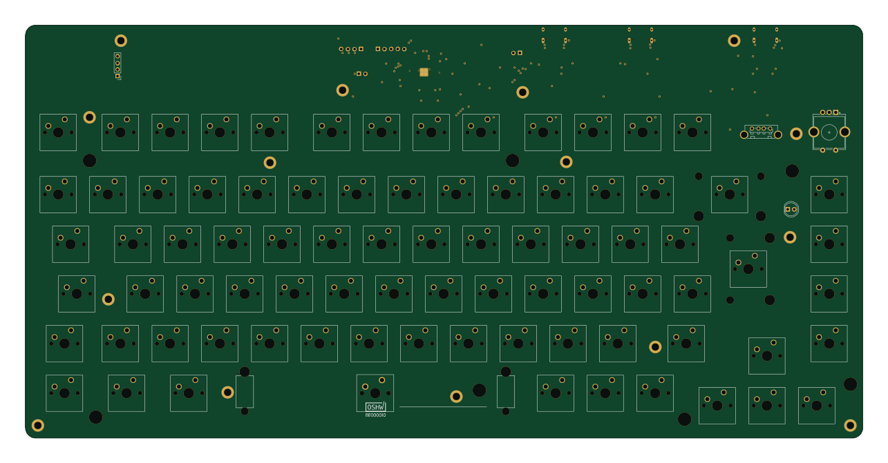 RP2040/RP2350
Quanta Keyboard PCB (Bare RP2040 JLCPCBA optimized)
320.7 × 158.3 mm234 parts2LCERN-OHL-P-2.06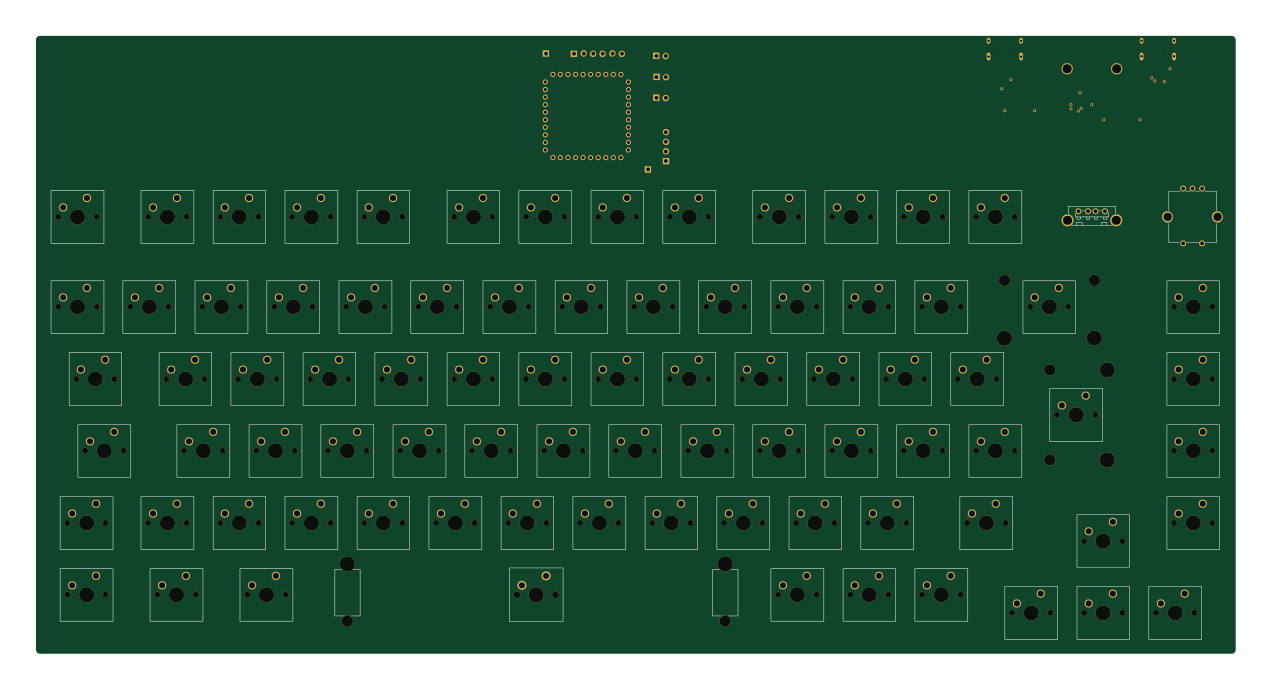 RP2040/RP2350
Quanta75 RP2040Stamp
317.5 × 163.5 mm216 parts2LCERN-OHL-P-2.06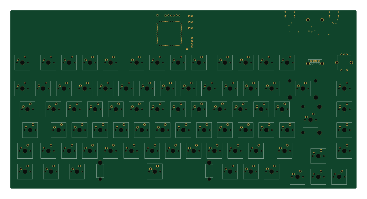 RP2040/RP2350
Quanta75 Pico
317.5 × 163.5 mm216 parts2LCERN-OHL-P-2.06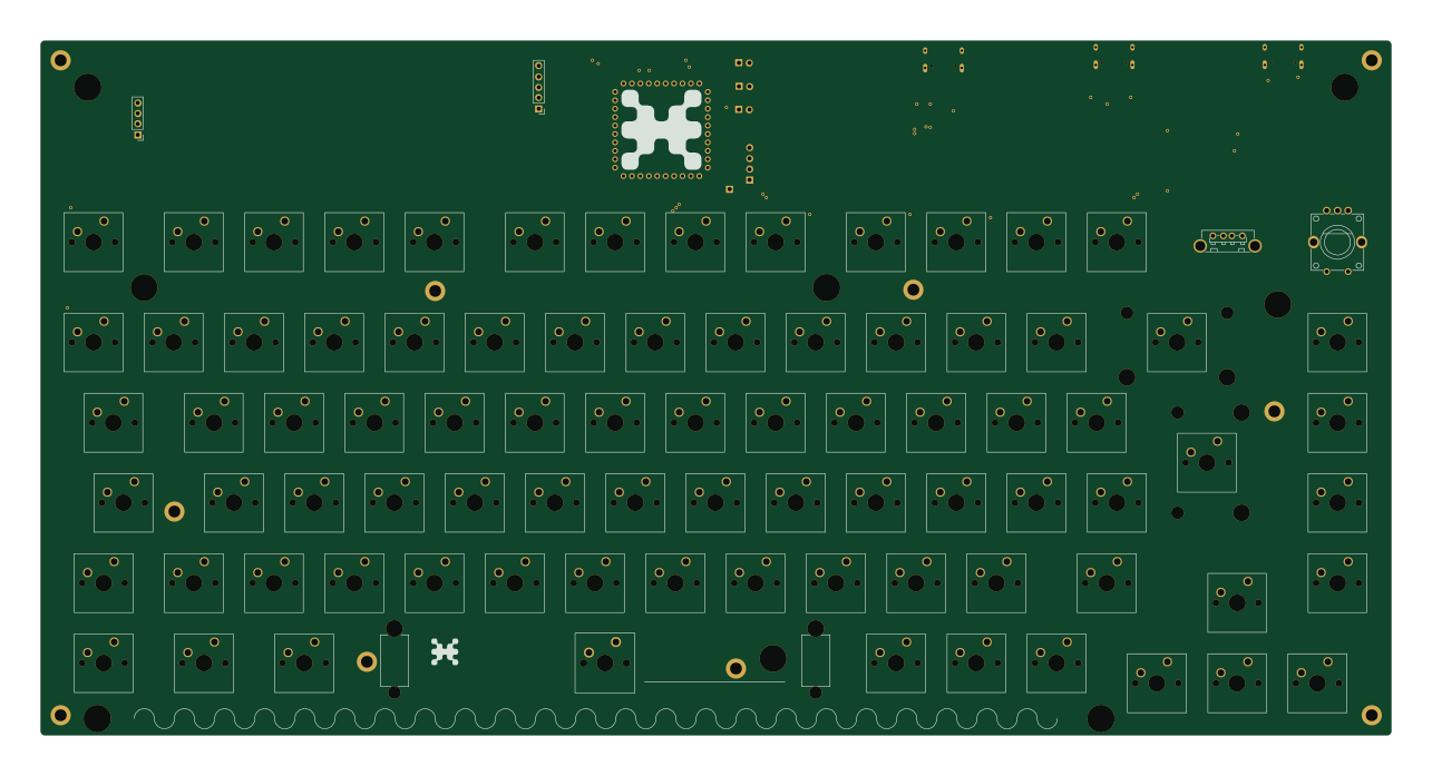 RP2040/RP2350
Quanta75 RP2040Stamp JLCPCBAoptimized.stretch bkup
320.7 × 165.1 mm214 parts2LCERN-OHL-P-2.06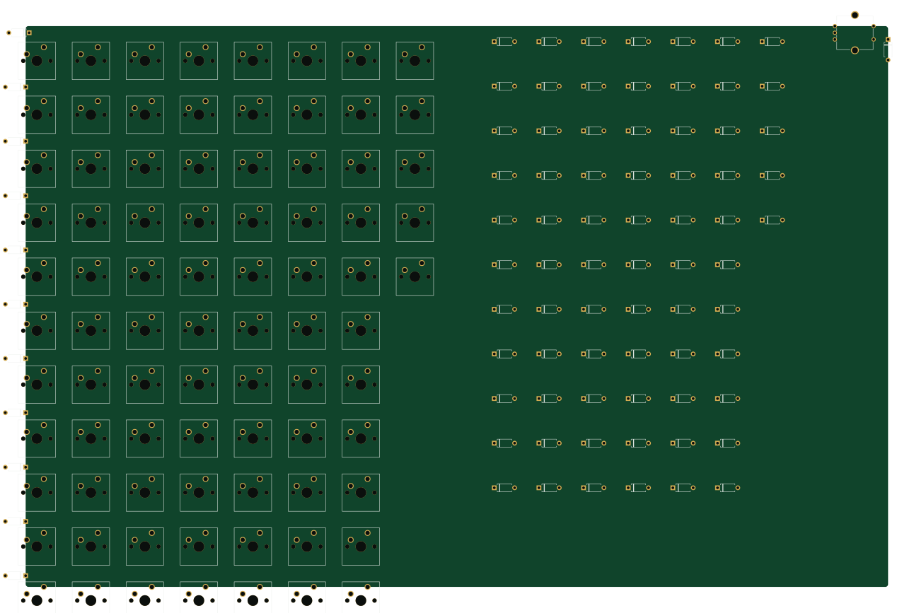
Quanta-ISO-Pico 01
322.6 × 209.9 mm166 parts2LCERN-OHL-P-2.06
Similar boards
 RP2040/RP2350
Open Book Abridged Edition
joeycastillo
85 × 115 mm29 parts2LCC-BY-SA-4.08.1k RP2040/RP2350
Corne
foostan
277.2 × 107.5 mm164 parts2LCC-BY-4.07.7k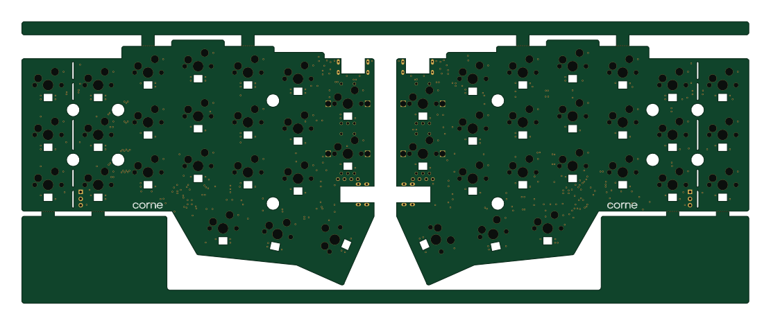 RP2040/RP2350
Corne
277.2 × 107.5 mm164 parts2LCC-BY-4.07.7k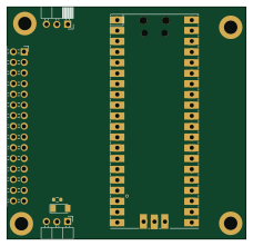 RP2040/RP2350
LogicAnalyzer
gusmanb
57 × 55.2 mm6 parts2LGPL-3.05.0k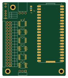 RP2040/RP2350
Jitx design
55.5 × 65 mm26 parts4LGPL-3.05.0k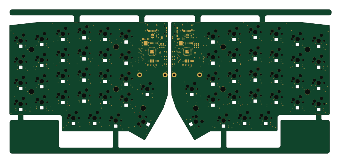 RP2040/RP2350
Pro V2
kata0510
290.1 × 130 mm270 parts2LMIT2.3k