
K6 coinbox daughter

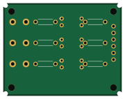
About the K6 coinbox daughter PCB
K6 coinbox daughter is an open source PCB design by opmedia-dev, published on GitHub. It is a 2-layer board measuring 45 × 35 mm, with 17 components from 17 distinct parts.
Other key parts include the PC817. By type, the board carries 6 resistors, 4 connectors and 3 ICs.
It belongs with the power & battery designs in this gallery.
From the project
KiCad 10 project for a 2-layer carrier board (100 × 100 mm). All modules plug in via through-hole pin headers — no SMD soldering required.
KiCad 10 project for a 2-layer carrier board (100 × 100 mm). All modules plug in via through-hole pin headers — no SMD soldering required.
See PINOUT.md for the complete pinout reference with every pin, net, and signal described.
1. Open the project in KiCad 10+ 2. File → Plot → select Gerber format, output to gerbers/ 3. Check layers: F.Cu, B.Cu, F.SilkS, B.SilkS, F.Mask, B.Mask, Edge.Cuts 4. Generate Drill Files → Excellon format 5. Zip the gerbers/ folder and upload to your fabricator
Main components on the K6 coinbox daughter
K6 coinbox daughter bill of materials (BOM)
17 components, 17 distinct parts.
| Qty | Part | Footprint | Refs |
|---|---|---|---|
| 1 | PC817 | U1 | U1 |
| 1 | PC817 | U2 | U2 |
| 1 | PC817 | U3 | U3 |
| 1 | COIN | J1 | J1 |
| 1 | BTN_A | J2 | J2 |
| 1 | BTN_B | J3 | J3 |
| 1 | TO_ESP32 | J4 | J4 |
| 1 | MH | MH1 | MH1 |
| 1 | MH | MH2 | MH2 |
| 1 | MH | MH3 | MH3 |
| 1 | MH | MH4 | MH4 |
| 1 | 470R | R1 | R1 |
| 1 | 470R | R2 | R2 |
| 1 | 470R | R3 | R3 |
| 1 | 10K | R4 | R4 |
| 1 | 10K | R5 | R5 |
| 1 | 10K | R6 | R6 |
K6 coinbox daughter design files
The KiCad project lives in the opmedia-dev/k6_gpo_exhibit repository on GitHub; these links point at the commit this page was built from.
K6 coinbox daughter: common questions
How big is the K6 coinbox daughter PCB?
The K6 coinbox daughter measures 45 × 35 mm, has 2 copper layers and is 1.6 mm thick.
How many components are on the K6 coinbox daughter?
17 components, from 17 distinct parts. The full bill of materials is listed on this page.
Where can I download the K6 coinbox daughter design files?
From the opmedia-dev/k6_gpo_exhibit repository on GitHub, which has the KiCad layout and the schematic; the links under Design files point to each one.
Can I use the K6 coinbox daughter design in my own project?
The repository has no license, so all rights stay with opmedia-dev. Use it as a reference, and ask the author before reusing the design.
More boards in k6_gpo_exhibit
Similar boards
EinkPDA screen
TalismanDesign
95 × 54 mm27 parts2LApache-2.02.0k
Stack chan
stack-chan
50 × 50 mm33 parts2LApache-2.01.7k
Display Carrier
AxxAxx
35.6 × 58.2 mm5 parts2LGPL-3.01.7k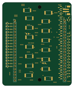
Module 16S PassiveBalanceAddOn
stuartpittaway
61 × 74 mm86 parts2LCC-BY-NC-4.01.1k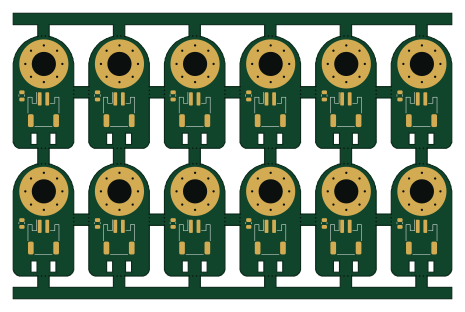
TemperaturePCB PANEL
116 × 75.5 mm178 parts2LCC-BY-NC-4.01.1k
ProgrammingAdapter
10.5 × 83 mm3 parts2LCC-BY-NC-4.01.1k