
GPS Clock Ver2


About the GPS Clock Ver2 PCB
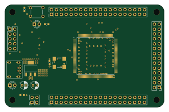
GPS Clock Ver2 is an open source PCB design by Otter-IO, published on GitHub under the GPL-3.0 license. It is a 2-layer board measuring 138.2 × 16.6 mm, with 5 components from 2 distinct parts.
It belongs with the rf & radio designs in this gallery.
From the project
FPGA Based GPS Synchronized Clock
The clock is split into 2 pieces, the FPGA board and the clock display. This was done so that to FPGA board could be used for other projects easily without redesign. It also allowed me to use a 4-layer board for the FPGA and a 2-layer board for the clock display. This helped keep costs low while also getting the advantages of a 4-layer board for the FPGA. The boards were designed using KiCAD.
GPS Clock Ver2 bill of materials (BOM)
5 components, 2 distinct parts — part numbers from the project's BOM.
| Qty | Part | Footprint | Refs |
|---|---|---|---|
| 1 | Conn_02x14_Odd_Even | PinHeader_2x14_P2.54mm_Vertical | J3 |
| 4 | 7_SEGMENT 7_Segment | 0.56_CC_7_Segment_Display | DS2, DS4, DS6, DS8 |
GPS Clock Ver2 design files
The KiCad project lives in the Otter-IO/GPS-Synchronized-Clock repository on GitHub; these links point at the commit this page was built from.
GPS Clock Ver2: common questions
How big is the GPS Clock Ver2 PCB?
The GPS Clock Ver2 measures 138.2 × 16.6 mm, has 2 copper layers and is 1.6 mm thick.
How many components are on the GPS Clock Ver2?
5 components, from 2 distinct parts, with part numbers taken from the project's own BOM. The full bill of materials is listed on this page.
Where can I download the GPS Clock Ver2 design files?
From the Otter-IO/GPS-Synchronized-Clock repository on GitHub, which has the KiCad layout and the BOM; the links under Design files point to each one.
Can I use the GPS Clock Ver2 design in my own project?
Yes, under the terms of its GPL-3.0 license, which Otter-IO chose for the repository.
More boards in GPS-Synchronized-Clock
Similar boards
Hat
pa3gsb
65 × 56 mm81 parts2LNo license675
Radioberry juice
65 × 56 mm87 parts2LNo license675
Radioberry preamp
65 × 56 mm137 parts2LNo license675
Hermes-Lite Small IO Expansion
softerhardware
18.4 × 12.5 mm6 parts2LNo license372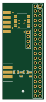
Hermes-Lite Jumper With IO
21.9 × 51.7 mm12 parts2LNo license372
Hermes-Lite PureSignal Feedback
17.1 × 15.4 mm6 parts2LNo license372