
Charge pump


About the Charge pump PCB
Charge pump is an open source PCB design by rmingon, published on GitHub. It is a 2-layer board measuring 10.2 × 9.1 mm, with 5 components from 4 distinct parts.
Other key parts include the ltc3240edc3.3. By type, the board carries 3 capacitors, 1 IC and 1 connector.
It belongs with the iot & wireless and power & battery designs in this gallery.
From the project
IOT - Ultra tiny 3.3V or 2.5V Step-Up/Step-Down Charge Pump DC/DC Converter
Thank you to PCBWay for sponsoring this project by covering the cost of PCB production for beta. The boards turned out very nicely. The green solder mask looks solid and the grills holes is perfect.
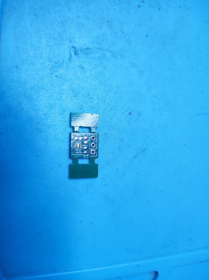
Main components on the Charge pump
Charge pump bill of materials (BOM)
5 components, 4 distinct parts.
| Qty | Part | Footprint | Refs |
|---|---|---|---|
| 1 | ltc3240edc3.3 LTC3240EDC-3_3 | DFN-6-1EP_2x2mm_P0.5mm_EP0.61x1.42mm | U1 |
| 1 | Conn_01x03 | PinHeader_1x03_P2.54mm_Vertical | J1 |
| 2 | 1uf | C_0603_1608Metric | C1, C3 |
| 1 | 4.7uf | C_0603_1608Metric | C2 |
Charge pump design files
The KiCad project lives in the rmingon/charge_pump repository on GitHub; these links point at the commit this page was built from.
- Layoutpcb.kicad_pcb
- Schematicpcb.kicad_sch
Charge pump: common questions
How big is the Charge pump PCB?
The Charge pump measures 10.2 × 9.1 mm, has 2 copper layers and is 1.6 mm thick.
How many components are on the Charge pump?
5 components, from 4 distinct parts. The full bill of materials is listed on this page.
Where can I download the Charge pump design files?
From the rmingon/charge_pump repository on GitHub, which has the KiCad layout and the schematic; the links under Design files point to each one.
Can I use the Charge pump design in my own project?
The repository has no license, so all rights stay with rmingon. Use it as a reference, and ask the author before reusing the design.
Similar boards

Stack chan
stack-chan
50 × 50 mm33 parts2LApache-2.01.7k
Display Carrier
AxxAxx
35.6 × 58.2 mm5 parts2LGPL-3.01.7k
ControllerCurrentShuntAddOn
stuartpittaway
26 × 16.9 mm9 parts2LCC-BY-NC-4.01.1k
Module 16S PassiveBalanceAddOn
61 × 74 mm86 parts2LCC-BY-NC-4.01.1k
TemperaturePCB PANEL
116 × 75.5 mm178 parts2LCC-BY-NC-4.01.1k
ProgrammingAdapter
10.5 × 83 mm3 parts2LCC-BY-NC-4.01.1k